India Developing Over 25 Chipsets with Homegrown IP

Synopsis
India is working on over 25 chipsets with indigenous IP to promote export-led growth in electronics. This initiative is supported by various projects and aims to enhance local manufacturing and design capabilities.
Key Takeaways
25 chipsets are in development using indigenous IP.
13 projects led by C-DAC in Bengaluru.
Government reforming semiconductor design across 300 organizations .
Target to create 85,000 skilled professionals .
New Centre of Excellence launched at NIELIT.
New Delhi, April 12 (NationPress) India is transitioning to an export-driven model in electronics and is actively developing more than 25 chipsets utilizing indigenous intellectual property (IP).
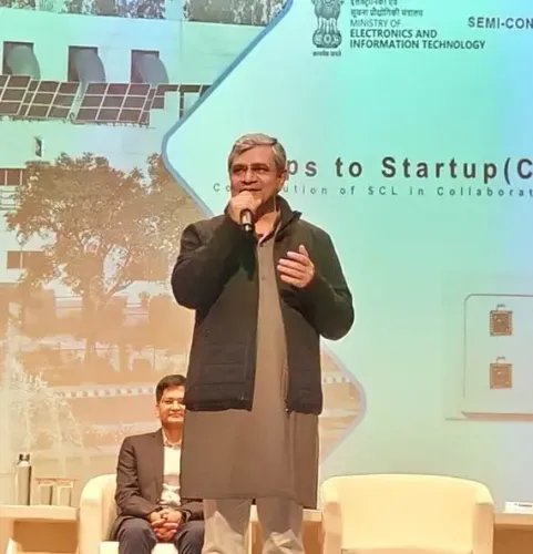
Union Minister for Railways and Electronics and IT, Ashwini Vaishnaw, revealed in a media briefing that 13 projects are currently in progress, spearheaded by the Centre for Development of Advanced Computing (C-DAC) in Bengaluru.
Holding intellectual property is crucial for ensuring security and shifting the country from a service-based economy to a product-oriented one, the minister stated, adding that upcoming semiconductor fabrication plants will produce these chips domestically.
To realize this vision, the government is systematically reforming the semiconductor design framework across over 300 organizations nationwide, including 250 academic institutions and 65 startups.
These initiatives are designed to usher in a new era of innovation, allowing anyone with the right skills, regardless of their location in the country, to design semiconductor chips, as per the IT Ministry. This aligns with Prime Minister Narendra Modi's vision that ‘Design in India is equally significant as ‘Make in India’.
The ‘Chips to Startup’ (C2S) program is structured to enhance every aspect of the electronics value chain through specialized workforce training, the establishment of a reusable IP repository, and the design of application-specific systems/ASICs/FPGAs, further supported by academia and R&D organizations leveraging the skills of startups and MSMEs.
The C2S program has a target of producing 85,000 industry-ready professionals at BTech, M.Tech, and PhD levels, specializing in semiconductor chip design. This initiative adopts a holistic approach, providing students with comprehensive hands-on experience in chip design, fabrication, and testing.
As part of the C2S program, a ‘ChipIN Centre’ has been established at C-DAC, serving as one of the largest facilities aimed at making chip design infrastructure accessible to the semiconductor design community across the nation.
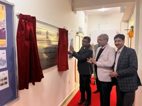
In February, a new Centre of Excellence (CoE) in chip design was inaugurated to meet the increasing demand for skilled professionals in the semiconductor and chip design sectors. This CoE was launched by the National Institute of Electronics and Information Technology (NIELIT) at its Noida campus.