How is IIT Madras Partnering with Applied Materials India to Enhance Semiconductor Innovation?

Synopsis
Discover how IIT Madras is teaming up with Applied Materials India to revolutionize semiconductor research. This partnership promises to accelerate innovation and workforce development in India’s semiconductor sector, positioning the country as a global leader in technology.
Key Takeaways
IIT Madras partners with Applied Materials India .
Implementation of the AppliedTwin digital twin framework.
Focus on enhancing semiconductor research and workforce development.
Planned semiconductor fabrication facility in Tamil Nadu.
Access to advanced tools for students and researchers.
New Delhi, Oct 23 (NationPress) The Indian Institute of Technology (IIT) Madras has officially revealed a collaboration with Applied Materials India to implement the AppliedTwin digital twin framework aimed at enhancing innovative semiconductor research and developing a skilled workforce.
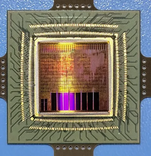
The AppliedTwin platform is an advanced digital twin solution crafted to simulate and optimize semiconductor manufacturing machinery and processes, as stated by the institute.
On the same day, a practical workshop focusing on AppliedTwin took place at IIT Madras, attracting over 150 participants, including students and faculty. Additionally, IIT Madras, in conjunction with the Tamil Nadu government, is working to set up a semiconductor fabrication facility that incorporates integrated reliability and packaging functions.
The introduction of the AppliedTwin digital framework at IIT Madras represents a significant advancement in fortifying India’s semiconductor research and development infrastructure while preparing a workforce equipped for industry demands, according to the announcement.
Prof. V. Kamakoti, Director of IIT Madras, highlighted that the AppliedTwin™ framework will enable both faculty and students to expedite concept generation, prototyping, testing, and process exploration in a virtual environment, leading to considerable reductions in research and development costs and timelines.
“By embedding state-of-the-art digital twin technologies into our educational programs and research initiatives, we strive to make significant contributions toward India’s ambition of becoming a global leader in semiconductor design and manufacturing,” Kamakoti expressed.
The foundational software supporting AppliedTwin™ is purposefully designed to encourage collaboration and construct an innovation network among suppliers, government entities, customers, and research institutions, thereby enhancing the development of India’s semiconductor ecosystem.
The software package provided to IIT Madras encompasses a multi-physics modeling tool, alongside TOPO+, a topography simulation tool.
Students from various institutions and MSMEs can access this software via the IITM platform, facilitated by Swayam Plus, as noted in the release.
With the provision of virtual semiconductor process experimentation, students and researchers will acquire practical insights into authentic fabrication workflows before India's physical FAB infrastructure becomes fully operational, according to the institute.
Point of View
The partnership between IIT Madras and Applied Materials India is a pivotal development in strengthening India's position in the global semiconductor landscape. It showcases a commitment to fostering innovation and building an industry-ready workforce, aligning with national priorities for technological advancement and economic growth.
NationPress
1 Jul 2026
Frequently Asked Questions
What is the purpose of the AppliedTwin framework?
The AppliedTwin framework is designed to model and optimize semiconductor manufacturing equipment and processes, enhancing research and development capabilities.
How will this partnership benefit students?
Students will gain access to virtualized semiconductor process experimentation, allowing them to understand real fabrication workflows and prepare for industry roles.
What is the significance of the semiconductor fabrication facility?
The facility will integrate reliability and packaging capabilities, significantly contributing to India's semiconductor ecosystem and technological self-reliance.