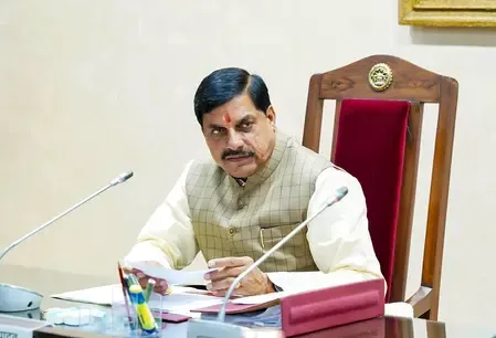
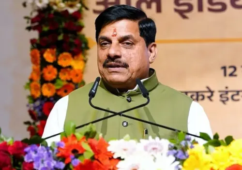
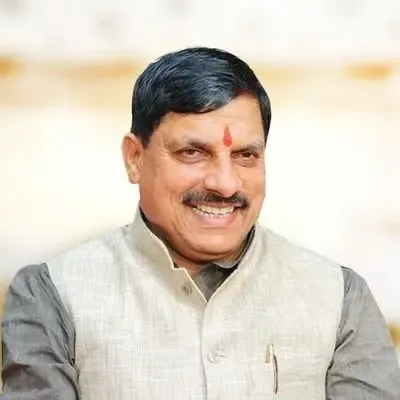
CM Mohan Yadav to launch MP Tech Growth Conclave 3.0 in Bhopal
Synopsis
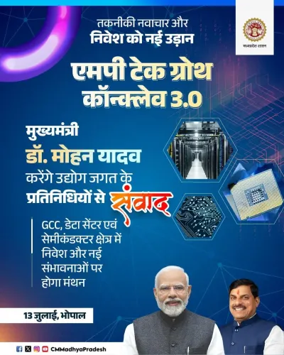
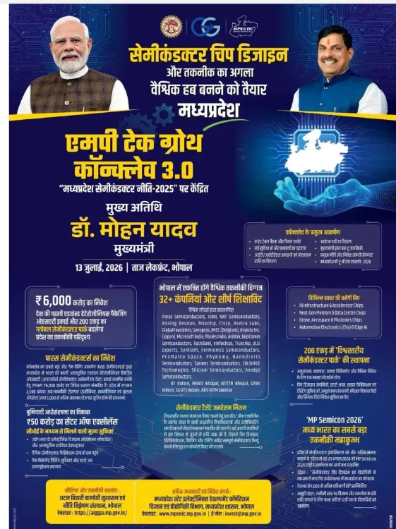
Chief Minister Dr. Mohan Yadav will inaugurate MP Tech Growth Conclave 3.0 in Bhopal on 13 July 2026, positioning Madhya Pradesh as India's next semiconductor chip design hub under the national India Semiconductor Mission framework. The MAPIT-organised summit marks the state's sharpest push yet into high-skill chip design investment.
Key Takeaways
Mohan Yadav will inaugurate MP Tech Growth Conclave 3.0 in Bhopal on 13 July 2026 .
Madhya Pradesh is positioning itself as the next global hub for semiconductor chip design and technology.
The conclave is the third edition of the state's recurring technology investment summit, organised by MAPIT .
The event aligns with India's India Semiconductor Mission , launched in 2021 to build a domestic semiconductor ecosystem.
Multiple Indian states are competing under the ISM framework to attract chip design firms and high-skill jobs.
Follow-up MoUs and state budget allocations for semiconductor training infrastructure are key markers to watch post-conclave.
Chief Minister Dr. Mohan Yadav is set to inaugurate the MP Tech Growth Conclave 3.0 in Bhopal on 13 July 2026, as Madhya Pradesh positions itself as the next global hub for semiconductor chip design and technology, according to a post by the official Chief Minister's Office account of the Government of Madhya Pradesh.
Context
The Chief Minister's Office announced on 13 July 2026 that CM Dr. Mohan Yadav will formally launch the third edition of the state's flagship technology summit. The post declared Madhya Pradesh as ready to become 'semiconductor chip design aur technology ka agla vaishvik hub' — 'the next global hub for semiconductor chip design and technology'. The conclave is organised by MAPIT (Madhya Pradesh Agency for Promotion of Information Technology), the state body responsible for IT policy implementation.
The MP Tech Growth Conclave is a recurring state-level summit, with each edition focused on attracting technology investment and showcasing the state's readiness for high-skill sectors. This third edition marks a sharper pivot toward semiconductor design, a domain that commands significant global attention and high-value employment.
Policy Backdrop
The conclave sits within the framework of India's India Semiconductor Mission (ISM), launched in 2021 under the Ministry of Electronics and Information Technology. The mission provides financial incentives for semiconductor design, fabrication, and assembly, and has catalysed inter-state competition to attract chip-related investments and talent.
Madhya Pradesh has been developing its IT and electronics sectors, leveraging its central geographic location and existing IT parks. The state's decision to anchor Conclave 3.0 around semiconductor design signals a deliberate escalation of its ambitions within the national semiconductor ecosystem, moving beyond general IT promotion toward a specialised, globally competitive segment.
Multiple Indian states have introduced targeted policies and investment summits under the ISM framework, aiming to reduce the country's heavy dependence on imported chips and to generate high-skill engineering employment at scale.
Stakeholders and Impact
The conclave is expected to draw semiconductor firms, IT companies, engineering graduates, and policy stakeholders. For Madhya Pradesh's large pool of engineering graduates, a successful push into chip design would open pathways into one of the world's highest-paying technology disciplines.
MAPIT will play a central coordinating role, as it does for state IT policy more broadly. Industry participants and potential investors attending the conclave will be watching for concrete policy commitments, infrastructure announcements, and any signals of state budget support for semiconductor training programmes.
What's Next
The immediate focus is on the 13 July 2026 inauguration by CM Dr. Mohan Yadav in Bhopal. Observers will look for follow-up announcements of memoranda of understanding with chip design companies, state-level incentive schemes, and any dedicated budget allocations for semiconductor skill development infrastructure.
If Madhya Pradesh secures credible investment commitments from this conclave, it would mark a significant step in the state's transition from a general IT destination to a specialised node in India's emerging semiconductor value chain — a shift that could define its technology identity for the decade ahead.
Point of View
Branding itself a semiconductor hub is a deliberate attempt to leapfrog from general IT services into a higher-value, more specialised segment — a strategy that carries both significant upside and execution risk. CM Mohan Yadav's personal inauguration signals that the state government views this as a political as well as economic priority. The real test will come in the months after the conclave, when investment pledges either translate into ground-level commitments or fade into the pattern of aspirational state-level summits.
NationPress
13 Jul 2026
Frequently Asked Questions
What is MP Tech Growth Conclave 3.0?
MP Tech Growth Conclave 3.0 is the third edition of Madhya Pradesh's state-level technology investment summit, focused on positioning the state as a global hub for semiconductor chip design. It is organised by MAPIT and will be inaugurated by Chief Minister Dr. Mohan Yadav in Bhopal on 13 July 2026.
Who is inaugurating MP Tech Growth Conclave 3.0?
Chief Minister Dr. Mohan Yadav will inaugurate MP Tech Growth Conclave 3.0 in Bhopal on 13 July 2026.
What is the India Semiconductor Mission?
The India Semiconductor Mission is a central government programme launched in 2021 under the Ministry of Electronics and Information Technology. It provides financial incentives for semiconductor design, fabrication, and assembly to build a domestic chip ecosystem and reduce import dependence.
Why is Madhya Pradesh focusing on semiconductor chip design?
Madhya Pradesh is targeting semiconductor chip design to attract high-value investment and high-skill jobs, leveraging its central location and existing IT parks. The move aligns with the national India Semiconductor Mission and the broader inter-state competition to become a node in India's emerging semiconductor value chain.