What Does the Cabinet's Approval of a Semiconductor Unit in UP Mean for Investment?
Synopsis
The Union Cabinet's recent approval for a semiconductor unit in Uttar Pradesh marks a significant investment opportunity. This facility, part of the India Semiconductor Mission, aims to enhance India's tech landscape and boost local manufacturing. With projected outputs reaching millions, it promises to support the growing demand in various sectors, aligning with the Atmanirbhar Bharat vision.
Key Takeaways
Cabinet approval for semiconductor unit Investment of Rs 3,700 crore Joint venture between HCL and Foxconn Located near Jewar airport Monthly production capacity of 20,000 wafers
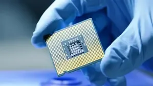
New Delhi, May 14 (NationPress) The Union Cabinet, led by Prime Minister Narendra Modi, has given the green light for the creation of a semiconductor facility in Uttar Pradesh as part of the India Semiconductor Mission (ISM), aiming to draw an investment of Rs 3,700 crore.
This facility is a collaboration between HCL and Foxconn, and it will be situated near Jewar airport in the Yamuna Expressway Industrial Development Authority (YEIDA) area.
The plant is expected to produce 20,000 wafers monthly, with a design output capacity of 36 million units each month. It will manufacture display driver chips for various devices including mobile phones, laptops, automobiles, PCs, and other display-enabled gadgets.
As outlined in a Cabinet note, the demand for semiconductors is surging alongside the rapid expansion of industries such as laptop, mobile phone, server, medical device, power electronics, defense equipment, and consumer electronics manufacturing in Bharat. This new unit will significantly contribute to Prime Minister Modi’s vision of ‘Atmanirbhar Bharat’.
With a rich history in hardware development and manufacturing, HCL teams up with global electronics giant Foxconn in this venture.
There are currently five semiconductor facilities in various stages of construction, and this sixth unit positions Bharat on a progressive path towards establishing a critical semiconductor industry, as noted by the Cabinet.
The semiconductor landscape is evolving rapidly across the nation, with world-class design facilities emerging in several states. State governments are actively engaging with design firms to foster growth.
Moreover, students and entrepreneurs from 270 academic institutions and 70 startups are focusing on cutting-edge design technologies for new product development. Approximately 20 products developed by students from these institutions have progressed to the tape-out stage at SCL Mohali.
As Bharat advances in its semiconductor journey, ecosystem partners are also setting up their operations in India. Major equipment manufacturers like Applied Materials and Lam Research have established a presence in the country. Additionally, suppliers such as Merck, Linde, Air Liquide, and Inox are preparing for the semiconductor industry's growth in India.
Point of View
It is crucial to recognize the implications of this Cabinet decision. The establishment of a semiconductor unit in Uttar Pradesh represents not just an investment, but a strategic move towards enhancing India's self-sufficiency in critical technology sectors. This aligns with national interests, fostering innovation and growth while positioning India as a competitive player in the global semiconductor arena.
NationPress
30 Jun 2026
Frequently Asked Questions
What is the investment amount approved for the semiconductor unit?
The investment amount approved for the semiconductor unit in Uttar Pradesh is Rs 3,700 crore.
Who are the joint venture partners for the semiconductor plant?
The semiconductor plant is a joint venture between HCL and Foxconn.
Where will the semiconductor unit be located?
The semiconductor unit will be located near Jewar airport in the Yamuna Expressway Industrial Development Authority (YEIDA) area.
What is the monthly production capacity of the plant?
The plant is designed to manufacture 20,000 wafers per month, with a design output capacity of 36 million units monthly.
How does this unit contribute to Atmanirbhar Bharat?
This unit supports the Atmanirbhar Bharat vision by enhancing local semiconductor manufacturing and reducing reliance on imports.