Is the HCL-Foxconn Plant a Sign of India's Semiconductor Manufacturing Maturity?
Synopsis
The recent Cabinet approval for the HCL-Foxconn chip plant signals a significant leap in India's semiconductor manufacturing capabilities. With an investment of Rs 3,700 crore, this facility aims to fill critical gaps in the electronics value chain, positioning India as a global semiconductor hub.
Key Takeaways
Investment: Rs 3,700 crore dedicated to the semiconductor plant.
Production Capacity: Designed for 20,000 wafers per month.
Global Expertise: Collaboration with Foxconn enhances manufacturing capabilities.
Strategic Importance: Fills critical gaps in India's electronics ecosystem.
Job Creation: Promises significant employment opportunities.
New Delhi, May 14 (NationPress) The recent approval by the Cabinet for the HCL-Foxconn chip manufacturing facility showcases India's evolving expertise in the semiconductor sector, according to industry analysts on Wednesday.
The Cabinet, led by Prime Minister Narendra Modi, sanctioned the setup of this semiconductor unit in Uttar Pradesh as part of the India Semiconductor Mission (ISM), which is expected to draw an investment of Rs 3,700 crore.
This decision represents a significant milestone in India's semiconductor journey, experts agree.
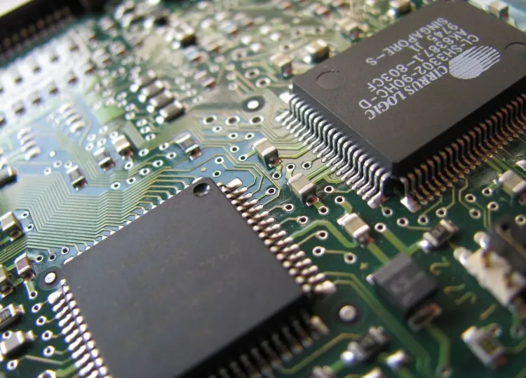
“With an investment of Rs 3,700 crore, the project will provide extensive advanced packaging and testing capabilities, particularly for display driver ICs, thereby filling a crucial void in India’s display and electronics ecosystem,” explained Ashok Chandak, President of IESA and SEMI India.
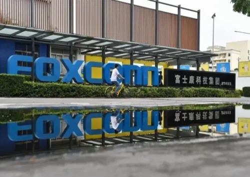
Foxconn, recognized as one of the globe’s leading electronics manufacturers, contributes its premier expertise in chip packaging and testing, essential for the downstream semiconductor supply chain.
Meanwhile, the HCL Group offers robust technology services, engineering prowess, and extensive global partnerships, enhancing local execution capabilities and talent acquisition.
“This collaboration establishes a foundation for India to become a favored global center for semiconductor OSAT (Outsourced Semiconductor Assembly and Test) operations, aligning with the 'Make in India' and 'Make for the World' initiatives, bolstered by strong support from both the Centre and state governments,” Chandak stated.
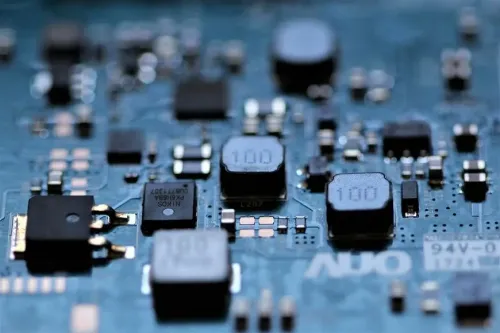
Located near Jewar airport, the plant is designed to handle 20,000 wafers monthly, with a production capacity of 36 million units per month. It will manufacture display driver chips for mobile phones, laptops, automobiles, PCs, and various other display-enabled devices.
“This initiative has the potential to become a landmark project, significantly enhancing value addition in India’s electronics manufacturing for sectors like mobile, laptop, consumer electronics, and automotive,” Chandak remarked.
With five semiconductor units already in advanced stages of construction, this sixth facility marks a pivotal step as “Bharat advances in its mission to build a strategically crucial semiconductor industry,” as stated by the Cabinet.
Point of View
The establishment of the HCL-Foxconn chip plant highlights India's commitment to becoming a key player in the global semiconductor landscape. This initiative not only promises substantial economic growth but also reinforces the importance of strategic partnerships in enhancing our technological capabilities.
NationPress
8 Jul 2026
Frequently Asked Questions
What is the significance of the HCL-Foxconn plant?
The HCL-Foxconn plant represents a strategic milestone for India, enhancing its semiconductor manufacturing capabilities and addressing critical gaps in the electronics value chain.
How much investment is being made in the project?
The project is backed by an investment of Rs 3,700 crore, aimed at developing advanced packaging and testing capabilities.
Where is the plant located?
The HCL-Foxconn chip plant is situated near Jewar airport in Uttar Pradesh.
What products will be manufactured at this facility?
The plant will manufacture display driver chips for mobile phones, laptops, automobiles, PCs, and other display-enabled devices.
How does this project align with India's broader economic goals?
This project aligns with India's 'Make in India' and 'Make for the World' initiatives, positioning the country as a preferred global hub for semiconductor operations.