Government Intensifies Efforts to Revamp Chip Design Framework
Synopsis
The Indian government is overhauling its semiconductor design approach across over 300 organizations, including 250 academic institutions and 65 startups, to democratize chip design and enhance local capabilities.
Key Takeaways
Government's initiative to revamp chip design.
Collaboration with over 300 organizations.
Focus on creating industry-ready professionals.
Establishment of ChipIN Centre for design support.
Development of indigenous semiconductor solutions.
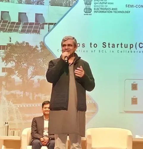
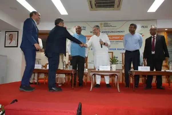
New Delhi, March 21 (NationPress) In a strategic move to establish chip design as a vital necessity, the government is initiating a comprehensive overhaul of the semiconductor design framework across over 300 entities nationwide — comprising 250 educational institutions and 65 startups.
As per the Ministry of Electronics and Information Technology (MeitY), these well-planned and proactive measures aim to usher in a new era of innovative empowerment, allowing individuals with inherent talents from any part of the nation to participate in semiconductor chip design.
In accordance with Prime Minister Narendra Modi's vision, chip design will be democratized, aligning with the belief that ‘Design in India is equally crucial as ‘Make in India’.
The C2S Programme is set to produce 85,000 industry-ready professionals at B.Tech, M.Tech, and PhD levels, specializing in semiconductor chip design,” the ministry stated.
The initiative adopts a holistic approach by providing students with extensive practical experience in chip design, fabrication, and testing.
This is facilitated through routine training sessions in partnership with industry stakeholders, along with mentorship and access to essential resources for chip design, fabrication, and testing, including EDA tools and semiconductor foundry access for chip production.
Participants will also engage in R&D projects aimed at developing functional prototypes of ASICs, SoCs, and IP Core designs.
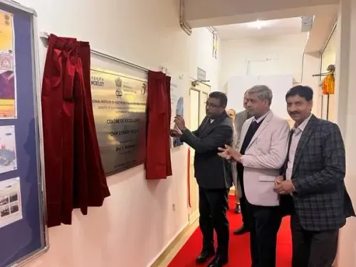
As highlighted by MeitY, the ChipIN Centre has been established under the C2S Programme as one of the largest facilities at C-DAC, designed to deliver chip design infrastructure directly to the semiconductor design community in the country.
In pursuit of its semiconductor mission, the indigenous development of the ‘BLDC Controller Chip’ has been entrusted to Vervesemi Microelectronics Pvt Ltd.
This ‘BLDC Controller Chip’ aims to achieve 90% of its BOM (bill of materials) sourced from India, providing a self-sufficient semiconductor solution with a complete power and control system priced under $1.50, and scalability of up to 10 million units annually, according to the ministry.
Vervesemi, a fabless semiconductor firm established in 2017, focuses on creating high-performance ASICs for sensors and wireless applications, leveraging state-of-the-art data converters and specialized Analog IP.