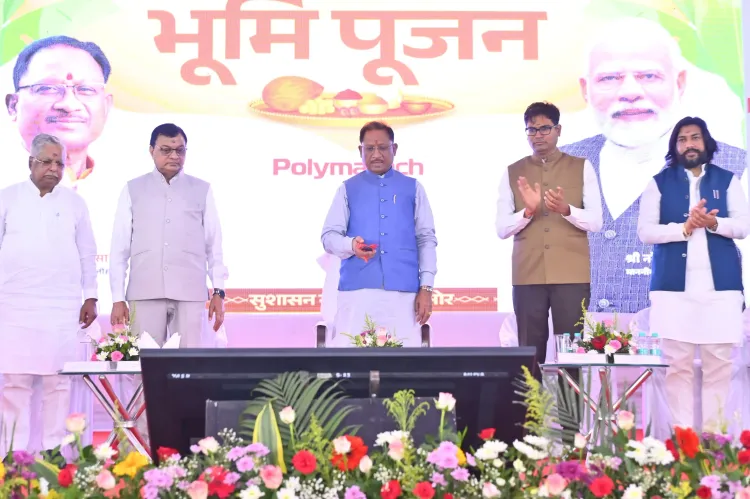
Chhattisgarh's First Semiconductor Plant Foundation Laid by CM Vishnu Deo Sai in Maoist-affected Region
Synopsis
On April 11, CM Vishnu Deo Sai laid the cornerstone for India's pioneering GaN-based semiconductor facility in Nava Raipur, aiming to empower local youth through technical training and create job opportunities, especially in Maoism-affected areas.
Key Takeaways
Foundation stone for India's first GaN semiconductor plant laid.
Focus on technical training for local youth.
Investment of Rs 10,000 crore announced.
Facility to produce 10 billion chips annually by 2030.
Supports Make in India and Digital India initiatives.
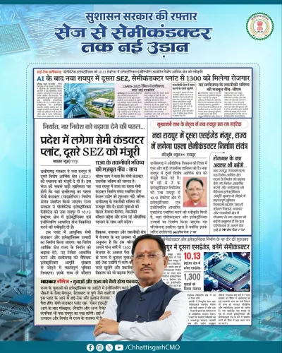
Nava Raipur, April 11 (NationPress) Chhattisgarh Chief Minister Vishnu Deo Sai officially inaugurated the foundation for the nation’s inaugural Ultra-edge technology-oriented Gallium Nitride (GaN)-based semiconductor fabrication facility in Nava Raipur.
“This is not merely a plant... it symbolizes the essence of a transformed Chhattisgarh,” remarked CM Sai, emphasizing that the most profound social changes will be observed in Bastar and other regions impacted by Maoism, where local youth will be integrated into this contemporary sector through technical training.
“Our goal extends beyond attracting investments; we aim to ensure that individuals from tribal, rural, and underdeveloped areas receive technical expertise and become vital contributors to India’s technological advancement,” he added, as per an official release.
During the occasion, the Managing Director of the firm establishing the unit revealed plans for an additional investment of Rs 10,000 crore in Chhattisgarh. He also announced that commercial operations are expected to commence by April-May 2026.
This cutting-edge facility, developed with an investment of Rs 1,143 crore, will manufacture high-frequency GaN chips designed to function between 5.925 GHz and 13.75 GHz (Nodes N102–104), serving advanced 5G and 6G telecommunications infrastructure, representing a significant milestone in India’s technological evolution.
The initiative is anticipated to generate considerable employment opportunities for local talent, attract foreign direct investment (FDI), and enhance regional economic growth.
The plant aims to produce 10 billion chips annually by 2030, potentially creating thousands of direct jobs and countless indirect employment opportunities, as per the statement.
This venture aligns directly with the Central Government's initiatives of 'Make in India' and 'Digital India', reducing reliance on imported semiconductors and fostering domestic innovation.
The company will manage the advanced packaging of these high-frequency chips at the Raipur facility, which will also act as a center for innovation in RF systems, defense electronics, artificial intelligence, data analytics, and high-performance computing.
Gallium Nitride is globally acknowledged as a superior choice to silicon for high-power, high-frequency applications due to its efficiency, thermal performance, and durability.
The establishment of this facility signifies India's entry into a high-value, strategic segment of the global semiconductor industry.
The statement indicated that the Chhattisgarh government has demonstrated its commitment to not only the 'ease of doing business' but also enhancing the 'speed of doing business'. The state administration acted promptly to ensure no obstacles hindered the establishment of this unit.
The Chhattisgarh government formalized an investment agreement with the company during the 'Chhattisgarh Investor Connect' event held in New Delhi in December 2024.
As per officials from the Industry Department, the company was allocated land in Sector 5 of Nava Raipur through a tender process in less than 45 days, and the lease deed registration was completed in under 25 days.