What Are the Implications of India's First 3nm Chip Design Centres?
Synopsis
Union Minister Ashwini Vaishnaw recently inaugurated two advanced design centers in India, marking a significant milestone in the semiconductor industry. With a focus on cutting-edge 3nm chip design, this initiative is set to elevate India's position in global tech innovation.
Key Takeaways
India's semiconductor industry is rapidly evolving .
New 3nm chip design facilities signify major technological advancement .
The initiative is part of a holistic semiconductor strategy .
Educational programs aim to enhance engineering skills .
Strong industry investments are being made .
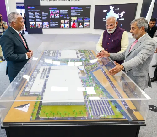
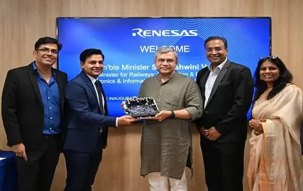
New Delhi, May 13 (NationPress) Union Minister for Electronics and IT, Ashwini Vaishnaw, inaugurated two state-of-the-art design centers of Renesas Electronics India in Noida and Bengaluru that will focus on advanced 3-nanometer chip design.
Vaishnaw highlighted that this achievement positions India prominently within the global semiconductor innovation landscape.
“Designing at 3nm is genuinely next-generation. We’ve previously achieved 7nm and 5nm, but this represents a groundbreaking advancement,” he stated.
The minister further elaborated on India's comprehensive semiconductor strategy, which includes design, fabrication, ATMP (Assembly, Testing, Marking, and Packaging), as well as supply chains for equipment, chemicals, and gases.
He pointed to the growing industry confidence reflected in global forums like Davos, mentioning considerable investments from firms like Applied Materials and Lam Research.
Emphasizing the growing momentum within India’s semiconductor ecosystem, he described the establishment of this significant Semiconductor Design Centre in Uttar Pradesh as a pivotal move towards creating a nationwide ecosystem that leverages the abundant talent across the nation.
“In merely three years, India’s semiconductor sector has evolved from a nascent stage to an emerging global hub, poised for sustainable long-term growth,” the minister asserted.
He also noted, “With the surge in manufacturing of electronic products such as smartphones, laptops, servers, medical devices, defense technology, and automobiles, the demand for semiconductors is set to increase dramatically. This growth momentum is incredibly timely.”
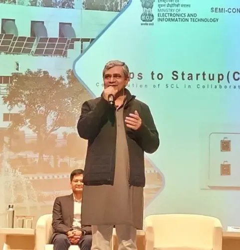
The minister also introduced a new semiconductor learning kit to enhance practical hardware skills among engineering students.
Over 270 academic institutions that have already received advanced EDA (Electronic Design Automation) software tools under the India Semiconductor Mission will also be provided these hands-on hardware kits.
“This fusion of software and hardware education will cultivate truly industry-ready engineers. We are not only developing infrastructure but also investing in the long-term growth of talent,” he remarked.
Hidetoshi Shibata, CEO and MD of Renesas Electronics, mentioned that India serves as a strategic cornerstone for their operations, with increasing contributions in embedded systems, software, and system innovation.
He emphasized Renesas' dedication to enhancing its end-to-end semiconductor capabilities in India, from architecture to testing, while aiding over 250 academic institutions and various startups through government-supported initiatives.
Point of View
The inauguration of the 3nm chip design centers marks a transformative step in India's technological evolution. By fostering innovation and attracting global investments, India is not only building infrastructure but is also nurturing a skilled workforce, ensuring that it remains competitive in the global semiconductor market.
NationPress
11 Jul 2026
Frequently Asked Questions
What is the significance of the 3nm chip design centres?
The 3nm chip design centres represent a significant advancement in semiconductor technology, positioning India as a key player in global tech innovation.
Where are the new design facilities located?
The new design facilities are situated in Noida and Bengaluru, India.
How does this impact India's semiconductor strategy?
This initiative enhances India's semiconductor strategy by integrating design, fabrication, and a comprehensive supply chain, accelerating the growth of the industry.
What educational initiatives are associated with this launch?
A new semiconductor learning kit will be introduced to improve practical hardware skills among engineering students, benefiting over 270 academic institutions.
Who is leading Renesas Electronics in India?
Hidetoshi Shibata is the CEO and Managing Director of Renesas Electronics and emphasizes India's strategic importance in their operations.