

MP CM Yadav Hands Over Land Letters at Indore Semiconductor Summit
Synopsis
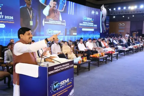
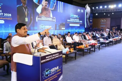
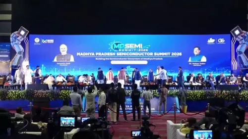
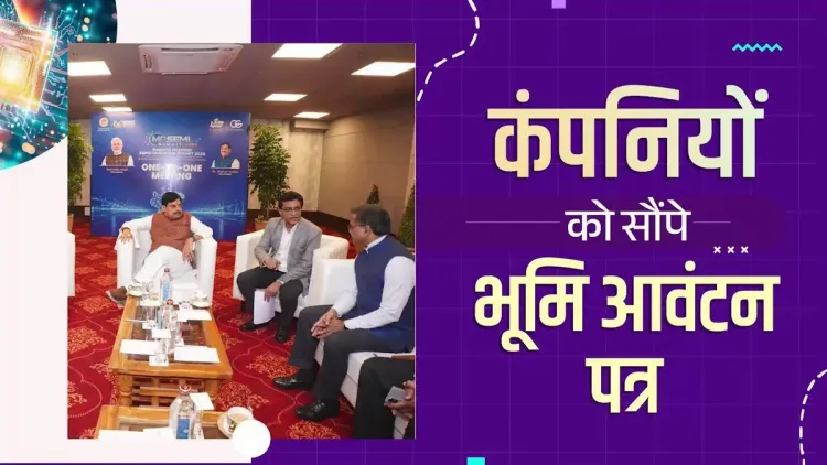
At the Semiconductor Summit in Indore on October 23, 2026, CM Dr. Mohan Yadav handed land allotment letters to participating companies, advancing Madhya Pradesh's push to attract chip-sector investment under India's national semiconductor self-reliance drive.
Key Takeaways
Mohan Yadav announced land allotment letters were formally handed to companies at the Semiconductor Summit in Indore on October 23, 2026 .
MAPIT and MPSeDC — the state's IT promotion and semiconductor development agencies — co-hosted and coordinated the summit.
Land allotment letters are a formal trigger for construction timelines, environmental clearances, and fiscal incentives for semiconductor projects.
The move aligns with the India Semiconductor Mission , launched in 2021 , which provides central incentives for chip fabrication and assembly.
Indore , MP's largest commercial city, was chosen as the host city, leveraging its existing industrial infrastructure and logistics connectivity.
Follow-up milestones to watch: ground-breaking announcements, environmental clearances, and conversion of allotments into active construction.
Semiconductor land is now in hand — literally. Chief Minister Dr. Mohan Yadav announced on Friday, October 23, 2026, that companies participating in the Semiconductor Summit in Indore have been formally handed land allotment letters, marking a concrete step toward establishing chip-related facilities in Madhya Pradesh.
Posting from the Chief Minister's Office account, CM Yadav stated: 'आज इंदौर में आयोजित सेमीकंडक्टर समिट में कंपनियों को भूमि आवंटन पत्र सौंपे गए हैं' — 'Today at the Semiconductor Summit held in Indore, land allotment letters have been handed over to companies.' The announcements were made in coordination with MAPIT (Madhya Pradesh Agency for Promotion of Information Technology) and MPSeDC (Madhya Pradesh Semiconductor and Electronics Development Corporation).What Land Allotment Letters Signal in Semiconductor Deals
A land allotment letter is not a ribbon-cutting — but it is the formal trigger that locks a company into a site and sets the clock running on construction timelines, environmental clearances, and fiscal incentives. For semiconductor projects, which require vast tracts of flat, stable, utility-rich land, getting this document in hand is a critical de-risking moment that separates intent from investable reality.
The summit in Indore — Madhya Pradesh's largest commercial city and a rising logistics corridor in central India — puts the state squarely in the frame of India's broader push to build domestic chip assembly, testing, and packaging capacity. Indore's existing industrial infrastructure and connectivity make it a logical anchor for this push.
MPSeDC, MAPIT, and the State's Chip Architecture
MPSeDC, the state's dedicated semiconductor and electronics development body, has been the institutional engine behind these outreach efforts, working alongside MAPIT to attract investment through land packages, policy support, and single-window clearances. Together, the two agencies represent Madhya Pradesh's twin-track approach: IT-sector broadening via MAPIT, and hard-infrastructure semiconductor play via MPSeDC.
Nationally, the India Semiconductor Mission, launched in 2021, set up central incentive structures — including capital support for fabrication and assembly units — to draw global chipmakers into the country. States have since raced to layer their own offers on top: land banks, power guarantees, and labour skilling pledges. Madhya Pradesh joins a cohort of proactive states marketing themselves as assembly-and-packaging destinations even as full-scale fab facilities remain concentrated elsewhere.
What Happens After the Letters Are Signed
The real test arrives in the months ahead. Land letters unlock the next phase: environmental impact assessments, utility connections, and the conversion of memoranda of understanding into actual ground-breaking ceremonies. CM Yadav's government will be watched closely on whether today's allotments translate into construction starts — the metric that separates a successful summit from a well-photographed one.
For Madhya Pradesh, getting companies to this stage is a signal that the state's semiconductor pitch is competitive. The question now is speed — how fast bureaucratic clearances follow the ceremony.
Point of View
Who took office in December 2023, the event is part of a pattern of state-level investment summits designed to signal investor confidence and generate tangible deliverables. The broader arc is clear: as India pursues semiconductor self-reliance through central incentives, states that can show speed of execution — not just attractive policy — will win the larger fabrication and packaging investments. Whether Madhya Pradesh can clear bureaucratic hurdles at the pace the sector demands will define the summit's legacy.
NationPress
23 Oct 2026
Frequently Asked Questions
What happened at the Indore Semiconductor Summit 2026?
At the Semiconductor Summit held in Indore on October 23, 2026, companies received formal land allotment letters from the Madhya Pradesh government, marking a key step toward setting up semiconductor facilities in the state.
What is MPSeDC and what does it do?
MPSeDC stands for Madhya Pradesh Semiconductor and Electronics Development Corporation. It is a state body focused on attracting semiconductor investments and facilitating land, policy support, and infrastructure for chip-related industries in MP.
What is the India Semiconductor Mission?
The India Semiconductor Mission was launched in 2021 by the central government to develop domestic chip design, fabrication, and assembly capabilities by offering capital support and incentives to attract global and domestic semiconductor companies.
Why is Indore chosen for the semiconductor summit?
Indore is Madhya Pradesh's largest commercial city and a major industrial and logistics hub in central India, making it a strategic location to host semiconductor investment events and attract companies looking for well-connected industrial sites.
What comes after the land allotment letters are handed over?
After receiving land allotment letters, companies typically proceed with environmental impact assessments, utility connections, and regulatory clearances before beginning construction — the key steps that convert summit commitments into active semiconductor projects.