

Andhra Pradesh semiconductor policy offers 80% subsidy, plans 5,000-acre chip park at Tirupati
Synopsis
Andhra Pradesh just made the boldest state-level semiconductor bet in India — an 80% combined subsidy for silicon fabs, outbidding Gujarat, Tamil Nadu and Odisha, backed by a 5,000-acre chip park at Tirupati and a single-window investor council chaired by the Chief Minister. If the park delivers on its infrastructure promises, it could become the anchor that pulls India's semiconductor supply chain southward.
Key Takeaways
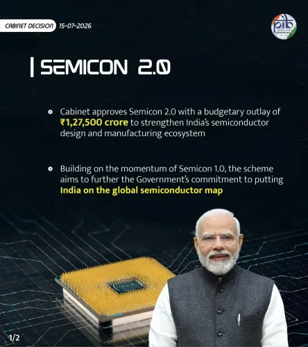
Andhra Pradesh amended its Semiconductor & Display Fab Policy 4.0 on 18 November 2026 to match the Centre's Semicon 2.0 capital support rupee for rupee.
Silicon fabs can now access 80% combined capital support — the highest among Indian states, ahead of Odisha and Tamil Nadu at 65%, UP and MP at 60%, and Gujarat at 56%.
A dedicated AP Semiconductor Park of approximately 5,000 acres is planned at Tirupati , offering shared cleanrooms, ultrapure water, high-voltage power, and on-site R&D facilities.
The APSGIC will act as a single-window clearance body, with an Oversight Council chaired by the Chief Minister .
Companies hiring trainees qualify for a ₹10,000 per trainee per month subsidy for six months under the AP-STCC .
Total state incentives are capped at 50% of eligible fixed capital investment ; combined support from all sources at 90% .
The Government of Andhra Pradesh has amended its Semiconductor & Display Fab Policy 4.0 to align with the second phase of the India Semiconductor Mission (ISM Semicon 2.0), matching the Centre's capital support rupee for rupee and announcing a dedicated 5,000-acre AP Semiconductor Park at Tirupati. The policy amendment, notified through a Government Order on 18 November 2026, positions Andhra Pradesh as the highest-incentive semiconductor destination among competing Indian states.
What the amended policy offers
Under the revised framework, a silicon fab approved under Semicon 2.0 can access combined capital support of 80 per cent of eligible capital cost — 40 per cent from the Government of India and a matching 40 per cent from Andhra Pradesh. Compound semiconductor, photonics, sensor, discrete and display fabs, and advanced packaging units are eligible for 70 per cent combined support, while legacy packaging units can access 50 per cent.
Assembly, Testing, Marking and Packaging (ATMP) and Outsourced Assembly and Test (OSAT) units will have 100 per cent of the Centre's capital support matched by the state. For R&D and talent projects, Andhra Pradesh contributes 25 per cent of eligible project cost, with combined Centre and state support capped at 75 per cent. Total state incentives are capped at 50 per cent of eligible fixed capital investment, and support from all sources at 90 per cent.
How Andhra Pradesh compares with rival states
The 80 per cent combined support for silicon fabs is higher than every other state currently competing for semiconductor investments — Odisha and Tamil Nadu offer 65 per cent, Uttar Pradesh and Madhya Pradesh offer 60 per cent, and Gujarat offers 56 per cent. This competitive edge, according to officials, is a deliberate strategy to attract anchor fabs that can catalyse a broader supplier ecosystem.
The amended policy covers all 10 Semicon 2.0 categories across six pillars: design, machines and materials, fabs, packaging, research and development, and talent. State support tranches are released on the same schedule as Centre disbursements.
The 5,000-acre semiconductor park at Tirupati
The planned AP Semiconductor Park, covering approximately 5,000 acres at Tirupati, is designed as a full-value-chain manufacturing and supplier cluster. It will be operated by a public-private park company with an investor-led board carrying up to three government nominees. The park will provide developed land, shared industrial cleanrooms, high-voltage power with redundancy, ultrapure water, natural gas and specialty gases, effluent treatment and water recycling, testing labs, logistics, and on-site research and training centres.
The AP Semiconductor Research & Innovation Centre (AP-SRIC), structured as a not-for-profit company with independent professional management, will anchor the research function. It will initially operate from IIT-Tirupati before relocating to the park, with photonics as its first area of focus.
Single-window clearance and talent development
The AP Semiconductor Growth & Innovation Council (APSGIC) will serve as a single point of contact for investors. It is governed by an Oversight Council chaired by the Chief Minister and an Apex Committee of experts that appraises projects, recommends state incentives, and coordinates clearances, land, power, water, and engagement with the ISM and the Union Ministry of Electronics and IT.
Workforce development is built into the framework through the AP Semiconductor Training & Capacity Building Centre (AP-STCC), housed within the park. Curricula will be co-designed with industry and Andhra Pradesh universities, and companies qualify for a training subsidy of ₹10,000 per trainee per month for six months.
Nara Lokesh, Minister for HRD, IT & Electronics, Government of Andhra Pradesh, said: 'Andhra Pradesh wants to be the place where India builds its chips, from design to fab to packaging. By matching the Centre's support rupee for rupee, giving investors one window and building the talent they need, we are making it simpler and cheaper to build a fab here than anywhere else in the country.'
What comes next
The launch of the semiconductor park project at Tirupati and the operationalisation of APSGIC will be watched closely by global chipmakers scouting India as an alternative to East Asian manufacturing hubs. With ISM Semicon 2.0 approvals underway at the Centre, the state's window to attract anchor investments is likely to narrow as competing states sharpen their own offers.
Point of View
And that is where most semiconductor ambitions have stalled before. The 5,000-acre park at Tirupati is an impressive commitment on paper, yet shared cleanrooms and ultrapure water supply at that scale require execution depth that few Indian state agencies have demonstrated. The single-window model under APSGIC is the right instinct, but its credibility will depend entirely on whether clearances actually move faster than in rival states. Andhra Pradesh is betting that outbidding on subsidy will attract the anchor investor that triggers an ecosystem; without that anchor, the park risks becoming expensive real estate waiting for a catalyst.
NationPress
18 Nov 2026
Frequently Asked Questions
What is Andhra Pradesh's amended Semiconductor & Display Fab Policy 4.0?
It is a revised state semiconductor incentive framework, amended in November 2026 to align with the Centre's India Semiconductor Mission Semicon 2.0. Under the amendment, Andhra Pradesh matches 100% of the Centre's capital support, giving silicon fabs a combined subsidy of up to 80% of eligible capital cost — the highest of any Indian state.
What is the AP Semiconductor Park planned at Tirupati?
It is a proposed 5,000-acre dedicated semiconductor manufacturing and supplier cluster at Tirupati, Andhra Pradesh. The park will be run by a public-private company with an investor-led board and will offer shared industrial cleanrooms, ultrapure water, high-voltage power, specialty gases, testing labs, logistics, and on-site research and training facilities.
How does Andhra Pradesh's semiconductor subsidy compare with other states?
Andhra Pradesh offers 80% combined capital support for silicon fabs, the highest among competing states. Odisha and Tamil Nadu offer 65%, Uttar Pradesh and Madhya Pradesh offer 60%, and Gujarat offers 56% under comparable schemes.
What is the APSGIC and how will it help semiconductor investors?
The AP Semiconductor Growth & Innovation Council (APSGIC) is a single-window body for semiconductor investors in Andhra Pradesh. It has an Oversight Council chaired by the Chief Minister and a CEO-led Apex Committee that appraises projects, recommends incentives, and coordinates land, power, water, and regulatory clearances in one place.
What training support does Andhra Pradesh offer semiconductor companies?
Andhra Pradesh will establish an AP Semiconductor Training & Capacity Building Centre (AP-STCC) inside the semiconductor park, with curricula co-designed by industry and state universities. Companies are eligible for a training subsidy of ₹10,000 per trainee per month for up to six months.