China chip packagers pour $2.2bn into AI capacity in H1 2026
Synopsis
China's top three chip packaging firms — JCET, Tongfu, and Huatian — have collectively pledged over $2.2 billion in H1 2026 to build AI chip assembly capacity, with JCET profits up 79.4% and Tongfu forecasting a staggering 337% profit surge, signalling a structural shift in the global semiconductor supply chain.
Key Takeaways
JCET , Tongfu Microelectronics , and Huatian Technology collectively announced capacity investments exceeding 15 billion yuan (US$2.2 billion) in the first half of 2026 .
JCET recorded a 79.4 per cent year-on-year net profit increase to 845 million yuan and a record revenue of 19.5 billion yuan in H1 2026 .
JCET unveiled a 7.8 billion yuan advanced packaging facility in Shanghai's Lingang area, with phase one due in the second half of 2028 .
Tongfu Microelectronics forecast a profit surge of up to 337 per cent year on year for H1 2026 , aided by its partnership with Advanced Micro Devices (AMD) .
Tongfu secured a 4.2 billion yuan private share placement approval, allocating 888 million yuan to add 849,600 wafers of annual memory chip capacity.
The expansion targets advanced packaging for AI accelerators , placing Chinese firms in direct competition with TSMC and ASE Technology Holding .
China's three dominant outsourced semiconductor packaging and testing companies — Jiangsu Changjiang Electronics Technology (JCET), Tongfu Microelectronics, and Huatian Technology — have collectively committed more than 15 billion yuan (US$2.2 billion) to capacity expansion in the first half of 2026, riding a wave of artificial intelligence demand and Beijing's accelerating push for domestic tech self-sufficiency.
Record earnings drive the buildout
JCET, China's largest chip packaging and testing firm, reported a 79.4 per cent year-on-year surge in net profit to 845 million yuan in the first half of 2026, with revenue hitting a record 19.5 billion yuan, according to its earnings report released last week. The growth was attributed to strong computing electronics sales, reflecting the broader AI hardware boom that has supercharged demand for advanced semiconductor assembly services.
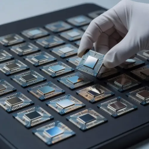
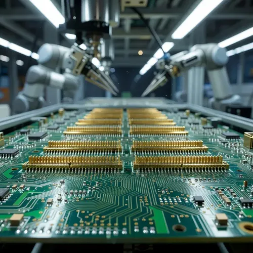
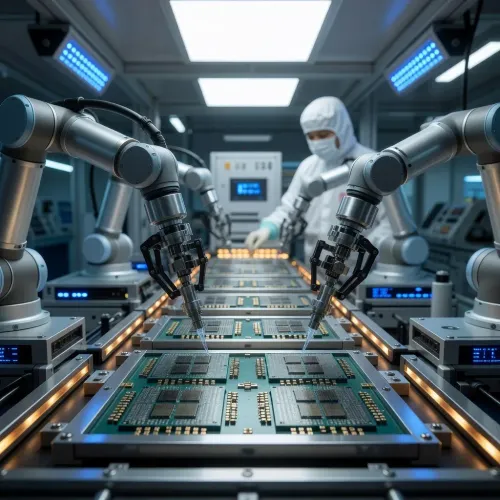
Packaging and testing represent the final critical steps in chip manufacturing, and the fresh capital injection is specifically aimed at scaling high-end advanced packaging capabilities for AI accelerators — components at the heart of systems powering large language models and data centre workloads.
JCET's Shanghai mega-facility
In June 2026, JCET unveiled a 7.8 billion yuan plan to construct a sprawling advanced packaging and testing facility in Shanghai's Lingang area, dedicated to high-end AI chips. Phase one of the project is scheduled for completion in the second half of 2028. The Lingang site, a designated free-trade zone, has become a focal point for China's semiconductor self-reliance strategy.
Tongfu's AMD partnership and capital raise
Tongfu Microelectronics — slated to release its latest earnings results on Friday — has forecast a first-half profit surge of up to 337 per cent year on year, driven partly by its strategic partnership with US semiconductor firm Advanced Micro Devices (AMD) on next-generation processors. The company recently secured regulatory approval for a 4.2 billion yuan private share placement, with 888 million yuan earmarked to add 849,600 wafers of annual memory chip capacity.
The AMD-Tongfu tie-up illustrates a nuanced dynamic in the global chip supply chain: even as geopolitical tensions restrict leading-edge chip exports to China, packaging partnerships between US design firms and Chinese assemblers continue to operate in a grey zone, providing both sides with strategic value.
The competitive backdrop
The expansion puts JCET, Tongfu, and Huatian on a direct collision course with Taiwan Semiconductor Manufacturing Company (TSMC) and ASE Technology Holding — the world's largest packaging and testing firm — in the advanced packaging segment. Technologies such as CoWoS (Chip-on-Wafer-on-Substrate), pioneered by TSMC for Nvidia AI chips, remain a benchmark that Chinese firms are racing to match or replicate domestically.
Smaller players such as SJ Semiconductor, based in Nanjing, are also investing in advanced packaging, widening the competitive field within China itself.
What's next
With Tongfu's earnings due Friday and JCET's Lingang facility entering its construction phase, the second half of 2026 will test whether domestic AI chip demand — and export-constrained foreign partnerships — can sustain the sector's extraordinary growth trajectory. Investors and industry watchers should monitor whether Huatian Technology's expansion announcements, and any further moves by China Securities-backed financing vehicles, signal a broader state-directed acceleration of the packaging buildout.
Point of View
Where restrictions are softer and partnerships with Western chip designers like AMD remain viable. The extraordinary profit multiples being reported, particularly Tongfu's forecast of up to 337 per cent profit growth, reflect not just AI demand but also the structural windfall from being one of the few credible alternatives to Taiwanese and South Korean assemblers. What mainstream coverage underweights is the dual-use nature of advanced packaging: the same CoWoS-class technologies that serve AI accelerators are equally critical to high-bandwidth military and aerospace applications, making this buildout geopolitically significant beyond its commercial headlines. Investors in ASE Technology Holding and TSMC's packaging segment should treat this as a medium-term competitive threat, not a distant one.
NationPress
26 Aug 2026
Frequently Asked Questions
How much are China's chip packaging companies investing in 2026?
China's three leading chip packaging firms — JCET, Tongfu Microelectronics, and Huatian Technology — announced combined capacity expansion investments exceeding 15 billion yuan (US$2.2 billion) in the first half of 2026. The capital is focused on advanced packaging for AI accelerators.
Why is JCET building a new facility in Shanghai's Lingang area?
JCET unveiled a 7.8 billion yuan plan in June 2026 to build an advanced packaging and testing facility in Shanghai's Lingang free-trade zone, specifically targeting high-end AI chips. Phase one is scheduled for completion in the second half of 2028, aligning with surging domestic and global demand for AI hardware.
What is Tongfu Microelectronics' connection to AMD?
Tongfu Microelectronics has a strategic partnership with US chip designer Advanced Micro Devices (AMD) focused on next-generation processors, which has been cited as a key driver of its forecast profit surge of up to 337 per cent year on year for H1 2026. The tie-up highlights how US chip designers and Chinese assemblers continue to collaborate even amid broader export restrictions.
How does China's packaging expansion affect TSMC and ASE Technology?
China's buildout directly challenges TSMC and ASE Technology Holding — the world's largest chip packaging firm — in the advanced packaging segment. Chinese firms are working to replicate or match technologies like TSMC's CoWoS, which is central to packaging Nvidia AI chips, intensifying competition in a segment previously dominated by Taiwanese players.
Why is advanced chip packaging important for AI?
Advanced packaging is the final step in chip manufacturing and is critical for AI accelerators because it enables multiple chips to be integrated at high density, boosting performance and bandwidth. Technologies like CoWoS allow memory and compute dies to be stacked closely, which is essential for the high-throughput demands of AI model training and inference.