JCET to invest $1.15bn in Shanghai advanced chip packaging plant

Synopsis
JCET is spending US$1.15 billion on a new Shanghai advanced packaging plant — a direct bet that China's AI chip boom will outlast US export controls and that domestic packaging capacity, not foundry access, is now the decisive competitive lever.
Key Takeaways
Jiangsu Changjiang Electronics Technology (JCET) will invest 7.8 billion yuan (US$1.15 billion) in a new chip-packaging and testing plant in Shanghai .
A controlled subsidiary with registered capital of 4 billion yuan will be set up to execute the project in the Lin-gang Special Area .
Phase one — factory construction and equipment procurement — is targeted for completion in the second half of 2028 .
JCET 's Shanghai -listed shares have risen 147 per cent since the start of 2026 , reflecting strong market confidence.
The investment is driven by surging domestic demand for AI -capable chips and Washington 's export controls limiting access to foundries such as TSMC .
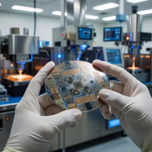
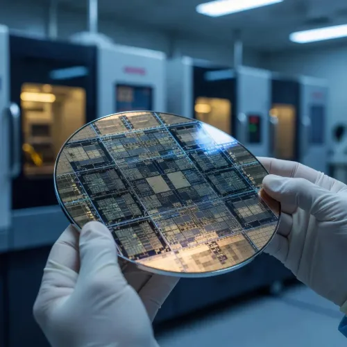
Jiangsu Changjiang Electronics Technology (JCET), China's largest chip-packaging and testing company, announced on Wednesday, 25 June 2026, that it will invest 7.8 billion yuan (US$1.15 billion) to construct a new advanced packaging and testing facility in Shanghai, as domestic demand for AI-capable chips accelerates. The investment underscores how advanced packaging has become a strategic priority for Chinese chipmakers navigating tightening US export controls.
The announcement
According to the company, a controlled subsidiary with a registered capital of 4 billion yuan will be established to develop an advanced packaging and testing factory in the Lin-gang Special Area in Shanghai. The project is structured in two phases, with the first phase — covering factory construction and equipment investment — scheduled for completion in the second half of 2028.
JCET, headquartered in Jiangsu province in eastern China, said the move is aimed at accelerating the expansion of its 'high-end' advanced-packaging capacity and enhancing the company's overall competitiveness, the company said.
Why it matters
Advanced packaging — the final stage of chip production that assembles individual dies into finished products — has emerged as a critical battleground for China's semiconductor industry. As Washington's export controls increasingly restrict Chinese firms' access to leading-edge foundries such as Taiwan Semiconductor Manufacturing Company (TSMC), domestic players are doubling down on packaging technology to extract more performance from chips they can still manufacture.
The rapid expansion of artificial intelligence infrastructure across China has intensified demand for home-grown chips, making advanced packaging capacity a direct enabler of the country's AI ambitions. JCET's new facility positions it to serve both domestic chip designers and global customers seeking supply-chain diversification.
Market reaction
JCET's Shanghai-listed shares have surged 147 per cent since the beginning of the year, reflecting strong investor confidence in the company's growth trajectory. The scale of this rally signals that markets are pricing in sustained, long-term demand for advanced packaging services well beyond the current AI investment cycle.
The competitive backdrop
The global advanced packaging market is intensely competitive, with TSMC's CoWoS and Samsung's advanced packaging lines dominating high-end AI chip assembly. JCET's $1.15 billion commitment signals a deliberate push to close the gap, particularly as Chinese fabless chip designers — cut off from leading-edge foundry access — increasingly rely on sophisticated packaging to boost chip performance.
What's next
The completion of the first phase by the second half of 2028 will be a key milestone to watch, as it coincides with what analysts expect to be a peak period for AI data-centre buildout in China. How quickly JCET can ramp capacity and attract anchor customers — particularly domestic AI chip designers — will determine whether this investment translates into durable market share gains.
Point of View
Packaging becomes the performance frontier. What mainstream coverage underplays is that advanced packaging — CoWoS-style chiplet integration, high-bandwidth memory stacking — can meaningfully compensate for a generation gap in process nodes, giving Chinese AI chip designers a viable path to competitive products. The 147 per cent share-price surge this year suggests investors already grasp this dynamic. The deeper risk, however, is equipment dependency: advanced packaging tools from firms like ASML and KLA remain subject to export licensing, meaning future US controls could target packaging equipment just as they have targeted lithography — a vulnerability JCET's capex plan does not yet publicly address.
NationPress
25 Jun 2026
Frequently Asked Questions
What is JCET's new Shanghai chip plant investment?
JCET is investing 7.8 billion yuan (US$1.15 billion) to build an advanced chip-packaging and testing factory in the Lin-gang Special Area of Shanghai . The project will proceed in two phases, with the first phase scheduled for completion in the second half of 2028 .
Why is advanced chip packaging important for China?
Advanced packaging is the final step in chip production, assembling individual dies into finished products, and has become critical to China 's semiconductor capabilities. As US export controls restrict Chinese firms' access to leading-edge foundries like TSMC , advanced packaging allows domestic chipmakers to boost performance without requiring the most advanced manufacturing nodes.
How have JCET shares performed in 2026?
JCET 's Shanghai -listed shares have surged 147 per cent since the beginning of 2026 . The rally reflects strong investor confidence in the company's growth prospects amid rising demand for AI-related chip services.
Where exactly will JCET build the new factory?
The new factory will be located in the Lin-gang Special Area in Shanghai , China . A controlled subsidiary with a registered capital of 4 billion yuan will be established specifically to construct and operate the facility.
How does JCET's investment compare to global rivals in advanced packaging?
JCET competes against advanced packaging operations run by Taiwan Semiconductor Manufacturing Company (TSMC) and Samsung , which currently lead in high-end AI chip assembly. The US$1.15 billion commitment signals JCET's intent to close the technology and capacity gap, particularly as Chinese fabless chip designers seek domestic alternatives to foreign packaging services.