China revises chip-design IP rules to fast-track semiconductor innovation
Synopsis
China's State Council, under Premier Li Qiang's decree, has revised integrated circuit layout-design protection rules effective October 15, 2026 — clarifying penalties, licensing, and co-ownership rights to fast-track chip commercialisation as US export controls tighten the screws on domestic fabrication.
Key Takeaways
Premier Li Qiang signed a State Council decree on August 3, 2026 , revising rules on the protection of integrated circuit layout designs.
The new regulations take effect on October 15, 2026 , and clarify financial penalties for IP infringement alongside licensing, transfer, and co-ownership rights.
Huawei Technologies is cited as a leading example of firms using hardware-software co-design to work around restrictions on advanced chipmaking equipment.
The revision aligns with China's 15th five-year plan (unveiled March 2026 ), which targets advances in mature-node processes, advanced fabrication, key equipment, and high-performance processors.
Domestic players including Naura Technologies and EDA firm Semitronix are among the companies operating in the ecosystem that stands to benefit from clearer IP rules.
China has overhauled its legal framework for protecting integrated circuit layout designs, a significant policy move aimed at accelerating semiconductor self-sufficiency as US export controls continue to squeeze access to advanced chipmaking equipment. Premier Li Qiang signed a State Council decree on Monday, August 3, 2026, promulgating the revised rules, which will take effect on October 15, according to Xinhua.
What the revised rules change
The updated regulations clarify financial penalties for intellectual property infringement and spell out licensing, transfer, and co-ownership rights for chip layout designs. The explicit codification of these provisions is intended to reduce legal ambiguity that has historically slowed the commercialisation of new designs developed by domestic firms.Why chip design matters in the semiconductor value chain
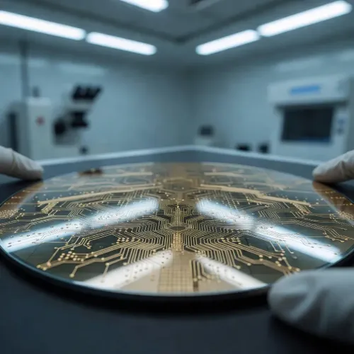
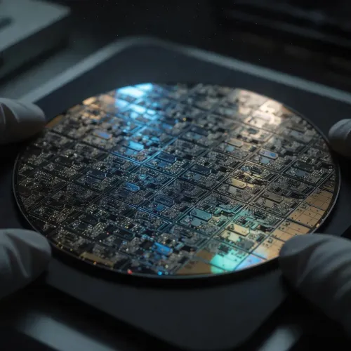
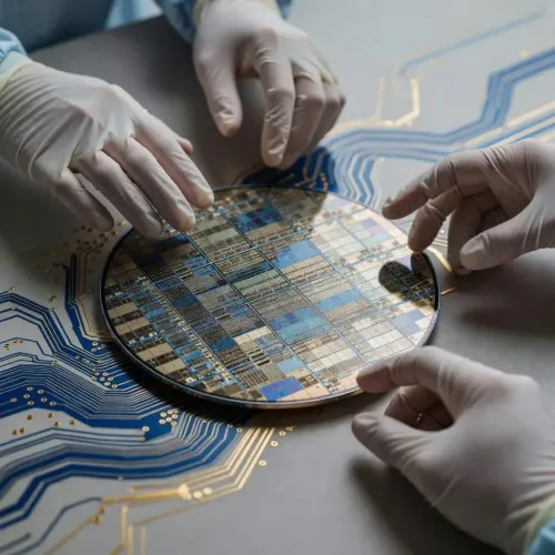
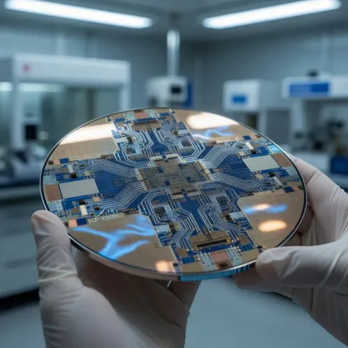
Chip design functions as the master blueprint for the entire semiconductor manufacturing process. While China's domestic fabrication capacity remains constrained by restrictions on importing advanced lithography and other equipment, expertise in chip design allows Chinese companies to innovate around production bottlenecks. Custom architectures — including the hardware-software co-design strategy that Huawei Technologies has publicly championed — represent a viable path to building competitive products without relying on leading-edge foundry processes.The five-year plan backdrop
The legal revision is directly aligned with Beijing's 15th five-year plan, unveiled in March 2026, which calls for efforts to 'refine and strengthen mature-node processes, enhance capabilities in advanced process technologies, accelerate development of key equipment, materials and components, and advance high-performance processors and high-density memory.' The IP update provides a commercial incentive layer to complement the plan's industrial targets.Competitive context
The move signals that Beijing is using regulatory tools — not just subsidies — to build out its semiconductor ecosystem. Firms across the domestic chip design landscape, as well as equipment makers such as Naura Technologies and EDA toolchain players like Semitronix, stand to benefit from clearer IP rules that make it easier to license and monetise proprietary designs. Stronger protections could also attract foreign co-investment into joint chip design ventures, provided geopolitical conditions permit.What's next
The rules take effect in October 2026, giving industry participants roughly ten weeks to align internal compliance processes. Analysts will watch whether the clarified co-ownership provisions unlock a new wave of joint design ventures between state-backed research institutes and private fabless firms. The broader test will be whether stronger IP protection translates into measurable acceleration of China's AI chip ecosystem — a benchmark that global semiconductor markets will be tracking closely.Point of View
Beijing is quietly building the contractual infrastructure needed to scale a fabless design ecosystem — the layer of the semiconductor stack where US export controls have the least direct bite. What mainstream coverage tends to underplay is the EDA angle: clearer IP rules make it commercially safer for domestic EDA toolchain providers like Semitronix to license their software broadly, reducing dependence on US-origin design tools that are themselves subject to export restrictions. If the October 2026 rules catalyse a wave of IP-sharing agreements between state research institutes and private fabless firms, China's chip design output could accelerate well ahead of its fabrication capacity — a structural shift that reshapes how the West thinks about the semiconductor chokepoint.
NationPress
18 Sept 2026
Frequently Asked Questions
What did China change about chip-design protection rules?
China revised its regulations on the protection of integrated circuit layout designs, clarifying financial penalties for infringement and spelling out licensing, transfer, and co-ownership rights. The State Council decree was signed by Premier Li Qiang on August 3, 2026, with the new rules set to take effect on October 15, 2026.
Why is China updating chip IP rules now?
The revision is part of Beijing's broader push for tech self-sufficiency under the 15th five-year plan unveiled in March 2026, as US export controls continue to restrict China's access to advanced chipmaking equipment. Stronger IP protections are intended to incentivise domestic firms to commercialise new chip designs more rapidly.
How does chip design help China work around US export controls?
Chip design — the architectural blueprint for semiconductors — is a layer of the value chain less directly constrained by US equipment restrictions than physical fabrication. Companies like Huawei Technologies are pursuing hardware-software co-design strategies to build competitive chips using available manufacturing processes.
Which Chinese companies are affected by the new chip-design rules?
The rules broadly affect China's domestic semiconductor ecosystem, including fabless chip designers, EDA toolchain providers such as Semitronix, and equipment makers like Naura Technologies. Clearer licensing and co-ownership provisions could also open the door to joint design ventures between state research institutes and private firms.
When do China's revised chip-design IP rules take effect?
The revised rules take effect on October 15, 2026, giving companies approximately ten weeks from the August 3 decree to prepare for compliance. Industry observers will be watching whether the new framework accelerates joint chip design activity and IP licensing deals across China's semiconductor sector.