Hwatsing Technology unveils China's first CMP-integrated 6-inch wafer metrology system
Synopsis
Hwatsing Technology has shipped China's first CMP-integrated six-inch wafer metrology system, enabling real-time in-line measurement during polishing — a quiet but strategically significant step in Beijing's push to reduce dependence on foreign semiconductor toolmakers.
Key Takeaways
Hwatsing Technology , based in Tianjin , announced a new metrology system for six-inch wafers on 7 August 2026 .
The system is China's first in-line measurement tool integrated directly with chemical mechanical polishing (CMP) equipment.
It enables real-time measurements before and after polishing, feeding live data back to the control system to improve process consistency.
The system has been shipped to an unnamed leading domestic optical silicon materials producer, marking its first commercial deployment.
The advance addresses inefficiencies in traditional production lines but does not close the gap with foreign leaders in advanced lithography, where ASML remains dominant.
China 's chip tool sector continues to make progress in sub-segments like CMP while remaining heavily dependent on overseas suppliers for more complex fabrication steps.
Hwatsing Technology, China's leading producer of chemical mechanical polishing (CMP) equipment, announced on Thursday, 7 August 2026 a new metrology system for six-inch wafers — marking the country's first in-line measurement tool paired directly with CMP equipment. The Tianjin-based company said the system has already been shipped to an unnamed leading domestic optical silicon materials producer, signalling early commercial traction.
What the breakthrough involves
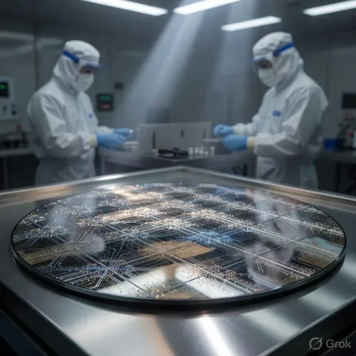
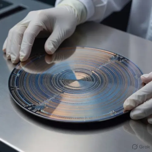
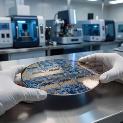
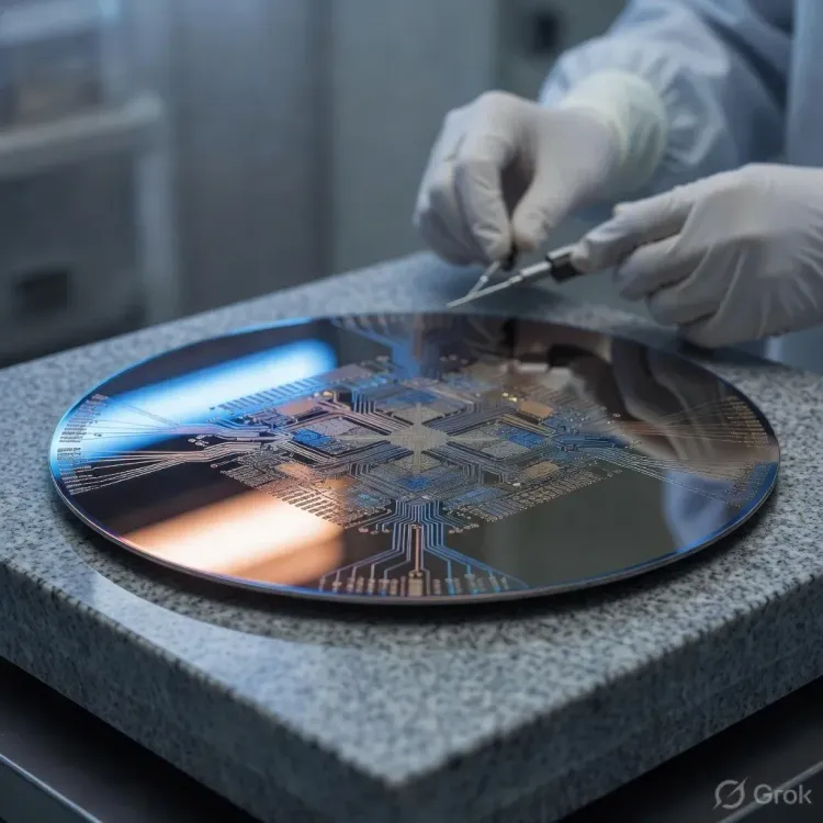
Wafers are thin, flat silicon discs that serve as the base for microchips, integrated circuits, and electronic devices. Transforming a raw wafer into a finished chip demands multiple precision steps — coating with photoresist, etching intricate layers, and wiring microscopic transistors — with polishing being a critical step that flattens and smooths the disc to exacting tolerances.
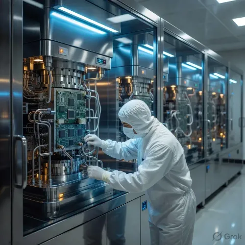
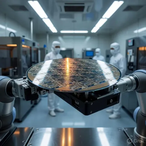
According to the company, the new metrology system integrates directly into the polishing workflow, enabling real-time measurements both before and after the polishing stage. Live data is fed back into the control system, allowing immediate process adjustments.
Why it matters
The direct integration of measurement and polishing into a single workflow could materially improve wafer uniformity and reduce material waste, the company said, addressing inefficiencies common in traditional, siloed production lines. For China's domestic semiconductor supply chain, which remains heavily reliant on foreign suppliers for more complex manufacturing tools, advances in CMP and metrology represent meaningful steps toward self-sufficiency in upstream chip fabrication.
CMP equipment and precision metrology sit at the intersection of multiple export-control pressure points, making domestic capability in these areas strategically significant beyond their immediate commercial value.
The competitive backdrop
While China has made incremental gains in wafer polishing and adjacent tooling, the industry continues to depend on overseas suppliers — most notably ASML of the Netherlands — for high-end photolithography systems used in advanced node production. Analysts at firms including Bernstein and Soochow Securities have tracked the widening gap between domestic Chinese toolmakers and global leaders in lithography, even as companies like Hwatsing close ground in sub-segments such as CMP.
The six-inch wafer segment, while less cutting-edge than the 300mm wafers used in leading-edge logic chips, is critical for power semiconductors, optical components, and legacy-node devices — all areas where China is aggressively expanding capacity.
What's next
The shipment to a domestic optical silicon materials producer suggests Hwatsing is targeting the materials supply chain as its first commercial beachhead for the new system. Broader adoption across wafer fabrication facilities would depend on the system's performance data from this initial deployment. Investors and industry observers will be watching whether Hwatsing extends the metrology platform to larger-diameter wafers — particularly 300mm — where the commercial and strategic stakes are considerably higher.
Point of View
Incremental gains in process steps that fall below the export-control radar, steadily reducing the number of foreign dependencies even where the headline lithography gap remains vast. CMP and metrology are not glamorous, but they are chokepoints — poor polishing uniformity cascades into yield losses across every subsequent fabrication step, so domestic capability here has outsized supply-chain value. What mainstream coverage often misses is that the six-inch wafer segment is not a consolation prize: it is the backbone of power electronics, compound semiconductors, and photonics, all of which are central to China's electric vehicle, defence, and telecoms industries. The real question is whether Hwatsing can leverage this metrology platform to move upmarket toward 300mm tools — and how quickly export-control regimes will respond if it does.
NationPress
21 Sept 2026
Frequently Asked Questions
What has Hwatsing Technology announced?
Hwatsing Technology announced on 7 August 2026 a new metrology system for six-inch wafers that integrates directly with its chemical mechanical polishing (CMP) equipment — the first such combined system in China . The tool enables real-time in-line measurement before and after polishing, feeding live data back to the production control system.
Why is this wafer polishing breakthrough significant for China?
The development is significant because it reduces China 's reliance on foreign suppliers for a critical semiconductor manufacturing step. CMP and precision metrology are essential to wafer uniformity and chip yield, and domestic capability in these areas strengthens the broader Chinese semiconductor supply chain amid ongoing export-control pressures.
What is chemical mechanical polishing and why does it matter?
Chemical mechanical polishing (CMP) is a manufacturing process that flattens and smooths silicon wafers to precise tolerances before and between chip fabrication steps. Without consistent polishing, subsequent processes — such as photolithography and etching — produce defective chips, making CMP a foundational step in semiconductor production.
Who is the customer for Hwatsing's new metrology system?
According to the company, the new system has been shipped to an unnamed 'leading domestic optical silicon materials producer' in China . The customer has not been publicly identified, but the shipment confirms the system has moved beyond development into early commercial deployment.
How does Hwatsing's advance compare to global chip tool leaders like ASML?
Hwatsing 's progress in CMP and metrology does not close the gap with global leaders in photolithography such as ASML , which supplies the extreme ultraviolet (EUV) machines needed for the most advanced chip nodes. China 's domestic toolmakers continue to make gains in specific process sub-segments while remaining dependent on foreign technology for high-end lithography.