China's basketball-sized diamond wafers could reshape AI chip cooling
Synopsis
Researchers at China's Harbin Institute of Technology have mastered a diamond-growing technique that could produce wafers as wide as a basketball — positioning China as a potential upstream gatekeeper for AI chip cooling materials at a moment when heat dissipation has become the binding constraint on semiconductor performance.
Key Takeaways
Harbin Institute of Technology (HIT) researchers led by Zhu Jiaqi have developed an MPCVD process capable of growing single-crystal diamonds of any size, up to a basketball-sized wafer.
On 31 May , HIT gifted one-carat lab-grown diamond rings to 187 doctoral student couples at its 11th group wedding , showcasing the technology's practical output.
Nvidia CEO Jensen Huang met Zhu Yanhui , founder of Chaoying Diamond Technology , during a January visit to Beijing , signalling global industry interest in China's diamond materials sector.
Diamond's exceptional thermal conductivity makes large synthetic wafers a potentially decisive material for dissipating heat in next-generation AI semiconductors.
Key Chinese industry players include Huanghe Whirlwind ( Sinomach Group ) and Nanjing Realway New Materials Technology , alongside academic spinouts from HIT .
The technology intersects with gallium nitride research, where diamond substrates are seen as critical for high-power semiconductor applications.
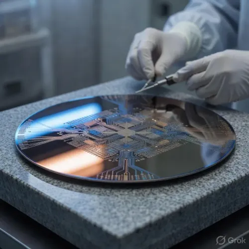
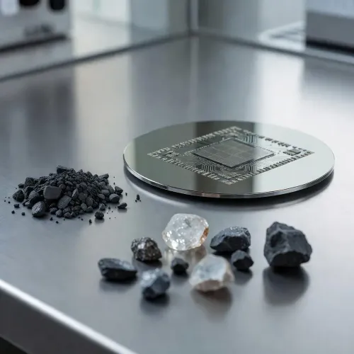
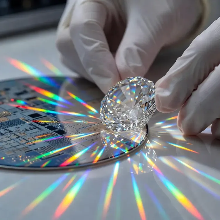
China is emerging as a global leader in ultra-large synthetic diamond production, with researchers at the Harbin Institute of Technology (HIT) developing a technique capable of growing high-purity, single-crystal diamonds of virtually any size — including wafers as wide as a basketball — a breakthrough that could prove critical to the next generation of AI hardware cooling.
The technology behind the breakthrough
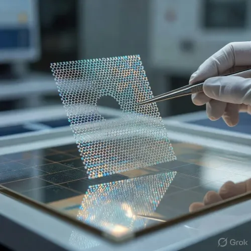
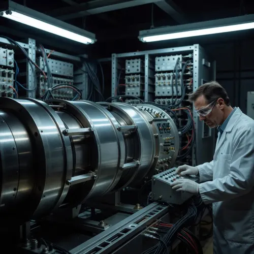
The process, known as microwave plasma chemical vapour deposition (MPCVD), generates carbon atoms in an ultra-clean environment and deposits them layer by layer onto a diamond seed crystal. The technique was developed by Zhu Jiaqi and his team from HIT's School of Astronautics, and is reportedly capable of producing diamonds of any shape and size — from gemstones to industrial-grade semiconductor wafers.
The scale of the achievement was on public display on 31 May when HIT held its 11th group wedding for doctoral students: each of the 187 newlywed couples received a one-carat diamond ring, with the stones grown in the university's own laboratory.
Why it matters for AI hardware
As the global AI race shifts from algorithmic competition to raw computing power, heat dissipation has become one of the most pressing physical constraints on chip performance. Diamond, with its unmatched thermal conductivity, is increasingly viewed as a material that could help semiconductor manufacturers break through this barrier.
A series of breakthroughs in growing large single-crystal diamonds could give China an unexpected structural advantage in next-generation AI hardware at a time when the country faces significant restrictions on accessing advanced chips from abroad.
The competitive backdrop
The strategic significance of the technology has not gone unnoticed at the highest levels of the industry. During a visit to Beijing in January, Nvidia chief executive Jensen Huang held a meeting with Zhu Yanhui, founder of Chaoying Diamond Technology, a supplier of diamond technology application materials, according to reports. The meeting underscored how seriously global chipmakers are taking diamond-based thermal solutions.
Other Chinese players active in this space include Huanghe Whirlwind, backed by Sinomach Group, and Nanjing Realway New Materials Technology. The broader ecosystem also intersects with gallium nitride semiconductor research, where diamond substrates are seen as a key enabler for high-power applications.
What's next
Researchers and industry observers are watching whether China's lead in MPCVD-grown diamond wafers can be translated into commercially viable semiconductor substrates at scale. If so, the country could hold a critical upstream position in the global AI chip supply chain — one that existing export controls do not currently address. The trajectory of companies like Chaoying Diamond Technology and the commercialisation pipeline out of institutions like HIT will be the key indicators to watch in the months ahead.
Point of View
The thermal substrate layer — where diamond could become as strategically important as high-bandwidth memory — has received far less scrutiny. The fact that Jensen Huang personally met a Chinese diamond materials founder during his January Beijing visit suggests that chipmakers are already stress-testing supply chain dependencies in this space. If MPCVD-grown diamond wafers reach commercial scale in China before Western producers, the next front in the semiconductor rivalry may not be about transistor density at all — it may be about who controls the heat.
NationPress
15 Sept 2026
Frequently Asked Questions
What is MPCVD diamond technology and why does it matter for AI?
Microwave plasma chemical vapour deposition ( MPCVD ) is a process that deposits carbon atoms layer by layer onto a diamond seed crystal in an ultra-clean environment, producing large, high-purity single-crystal diamonds. For AI hardware, this matters because diamond has exceptional thermal conductivity, making it a prime candidate for dissipating the intense heat generated by high-performance semiconductors — a problem that is increasingly limiting chip performance.
Who developed China's large synthetic diamond wafer technology?
Zhu Jiaqi and his team at the School of Astronautics , Harbin Institute of Technology (HIT) , developed the MPCVD -based technique. The team demonstrated the technology publicly when HIT presented one-carat lab-grown diamond rings to 187 doctoral student couples at its group wedding ceremony on 31 May .
Why did Jensen Huang meet a Chinese diamond company founder?
Nvidia CEO Jensen Huang met Zhu Yanhui , founder of Chaoying Diamond Technology , during a visit to Beijing in January , according to reports. The meeting reflects growing interest from global chipmakers in diamond-based thermal management materials as heat dissipation becomes a critical bottleneck in AI chip design.
Could China's diamond wafer lead give it an advantage in the AI chip race?
Potentially yes. If China can commercialise basketball-sized single-crystal diamond wafers at scale, it could control a key upstream material for next-generation AI semiconductors — one not currently targeted by Western export controls. Analysts note that heat management, not just transistor counts, is increasingly the binding constraint on AI computing performance.
Which Chinese companies are active in synthetic diamond semiconductor materials?
Key players include Chaoying Diamond Technology (founded by Zhu Yanhui ), Huanghe Whirlwind (backed by Sinomach Group ), and Nanjing Realway New Materials Technology . Academic research from Harbin Institute of Technology is also feeding into the commercial pipeline for diamond substrates used in gallium nitride and AI chip applications.