SK Hynix weighs $3bn sale of Chongqing chip plant in AI pivot
Synopsis
SK Hynix is reportedly weighing a stake sale of its Chongqing packaging plant at a ~$3 billion valuation — a move analysts say signals a decisive exit from low-margin NAND back-end work in favour of high-bandwidth memory for AI, even as chip-cycle volatility and US-China tensions complicate any deal.
Key Takeaways
SK Hynix confirmed on Monday, August 11, 2026 , that it is exploring options for its Chongqing packaging plant, including a potential stake sale valued at around US$3 billion .
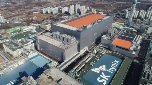
The Chongqing facility handles back-end packaging and testing for NAND flash memory; it is separate from SK Hynix 's front-end DRAM plant in Wuxi and NAND fab in Dalian .
Analyst Diana Wang of ICWise said profit growth in high-bandwidth memory (HBM) is 'far clearer than in standard NAND flash,' underpinning the strategic rationale.
Zhang Guobin , founder of eetrend.com , characterised the move as a shift 'from low-value back-end assembly to high-margin front-end manufacturing.' Potential Chinese buyers reportedly include Tongfu Microelectronics , Huatian Technology , JCET Group , Payton Technology , and YMTC .
SK Hynix stated no final decisions have been made, citing valuation hurdles and a volatile chip cycle as complicating factors.
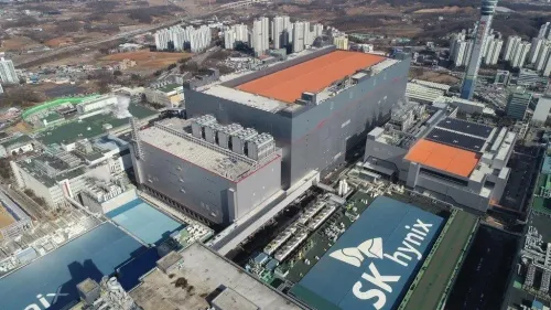
SK Hynix, the South Korean memory chip giant, is exploring options for its packaging facility in Chongqing, China, including a stake sale that could value the plant at around US$3 billion, as the company strategically redirects capital toward higher-margin artificial intelligence (AI) memory products. The company confirmed on Monday, August 11, 2026, that it is 'looking into various solutions to enhance the competitiveness of its packaging business,' though it stated no final decisions have been made.
What the Chongqing Plant Does
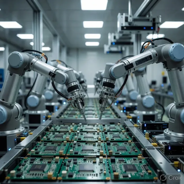
The Chongqing facility serves as a back-end hub for downstream packaging and testing of SK Hynix's NAND flash memory products. Unlike front-end wafer fabrication, back-end packaging is a lower-margin, labour-intensive process — precisely the segment the company appears eager to exit or restructure. SK Hynix separately operates front-end wafer fabrication plants in Wuxi (eastern China) for DRAM products and in Dalian (northeastern China) for NAND products, which are not part of the reported divestiture discussions.
Why It Matters: The AI Memory Shift
Industry analysts view the potential divestiture as a capital-recycling move away from commoditised legacy products. Diana Wang, an analyst at Chinese semiconductor research firm ICWise, noted that profit growth in high-bandwidth memory (HBM) — the memory architecture powering AI accelerators — is 'far clearer than in standard NAND flash.' HBM has emerged as one of the most lucrative segments in the global chip industry, with demand driven by AI training and inference workloads.
Strategic Backdrop: Low-Value to High-Margin
Zhang Guobin, founder of Chinese semiconductor news platform eetrend.com, described the move as a strategic shift 'from low-value back-end assembly to high-margin front-end manufacturing.' Potential acquirers for the Chongqing plant could include domestic Chinese packaging specialists such as Tongfu Microelectronics, Huatian Technology, JCET Group, or Payton Technology, all of whom operate in the back-end semiconductor services space. YMTC, China's state-backed NAND flash producer, has also been cited in industry discussions given its strategic interest in domestic packaging capacity.
Valuation Hurdles and Chip-Cycle Risk
Analysts cautioned that a transaction may not be straightforward. Navigating valuation expectations amid a volatile memory chip cycle — where NAND flash pricing has faced sustained pressure — could complicate negotiations. The deal also sits against a fraught US-China tech geopolitical backdrop, with foreign chipmakers facing increasing scrutiny over their China operations and investment flows. Any stake sale involving a major South Korean chipmaker and a Chinese buyer would likely draw regulatory attention from multiple jurisdictions.
What's Next
The outcome of SK Hynix's review of its Chongqing plant will be a closely watched signal for how foreign memory chipmakers intend to manage their China exposure as the industry's centre of gravity shifts toward AI-optimised memory. Investors and competitors alike — including Samsung and Micron, both of whom operate in China — will be monitoring whether a deal materialises and at what valuation, as it could set a precedent for further restructuring across the sector.
Point of View
Where it currently holds a commanding lead over rivals. What mainstream coverage underweights is the regulatory complexity — any sale to a Chinese domestic player like YMTC or JCET would face scrutiny not just from Seoul and Beijing, but potentially from Washington, given existing export-control frameworks targeting advanced semiconductor technology transfers. The ~US$3 billion valuation also looks ambitious in a NAND cycle that has yet to fully recover, suggesting the final price — if a deal closes at all — could disappoint. This episode is a microcosm of the broader dilemma facing non-Chinese chipmakers: how to monetise legacy China exposure without triggering geopolitical blowback or sacrificing strategic optionality.
NationPress
26 Sept 2026
Frequently Asked Questions
Why is SK Hynix selling its Chongqing chip plant?
SK Hynix is exploring a sale of its Chongqing packaging plant to redirect capital toward higher-margin AI memory products, particularly high-bandwidth memory (HBM) . The facility handles lower-margin back-end packaging for NAND flash, a segment analysts say offers far weaker profit growth than HBM .
How much is the SK Hynix Chongqing plant worth?
A potential stake sale could value the Chongqing plant at around US$3 billion , according to reports citing Bloomberg . SK Hynix has confirmed it is exploring options but said no final decisions have been made.
Who might buy the SK Hynix Chongqing facility?
Potential acquirers reportedly include Chinese semiconductor packaging firms Tongfu Microelectronics , Huatian Technology , JCET Group , and Payton Technology , as well as state-backed NAND producer YMTC . Any deal involving a foreign chipmaker and a Chinese buyer would likely face multi-jurisdictional regulatory review.
Does SK Hynix still operate other chip plants in China?
Yes. SK Hynix operates two front-end wafer fabrication facilities in China that are not part of the reported sale — a DRAM plant in Wuxi and a NAND fab in Dalian . Only the back-end packaging and testing plant in Chongqing is under review.
What is high-bandwidth memory (HBM) and why does SK Hynix want to focus on it?
High-bandwidth memory (HBM) is a specialised DRAM architecture used in AI accelerators and graphics processors, commanding significantly higher margins than standard NAND flash. SK Hynix is currently a leading HBM supplier to major AI chip customers, making it a core growth driver as demand for AI compute infrastructure surges globally.