India's semiconductor push: 12 projects, ₹1.64 lakh crore, 7 chips fabricated
Synopsis
India has crossed a critical threshold — from semiconductor policy to actual manufacturing. With 3 fabs in commercial production, 7 chips fabricated at nodes as advanced as 12 nm, and Semicon 2.0's ₹1,27,500 crore approved in July 2026, India is no longer just a design services destination. The question now is whether it can scale fast enough to compete with state-backed chip giants in the US, EU, and East Asia.
Key Takeaways
India has approved 12 semiconductor projects across six states , with investment commitments exceeding ₹1.64 lakh crore .
Seven chips have been successfully fabricated, including at advanced nodes such as 12 nm .
Three facilities have commenced commercial production as of August 2026 .
211 chips were taped out by 75 institutions by April 2026 .
Semicon 2.0 was approved in July 2026 with an outlay of ₹1,27,500 crore .
The IndiaAI Mission has expanded shared compute to over 45,000 GPUs ; 237 projects have accessed 93.18 lakh GPU hours of subsidised compute by August 2026.
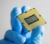
India is systematically building domestic capabilities across the semiconductor value chain — spanning chip design, fabrication, advanced packaging, equipment, and materials — with seven chips successfully fabricated at various process nodes, including advanced nodes such as 12 nm, according to an official government factsheet released on 14 August 2026. The disclosure underscores a decisive shift from policy announcements to on-ground manufacturing.
Scale of Semiconductor Investments
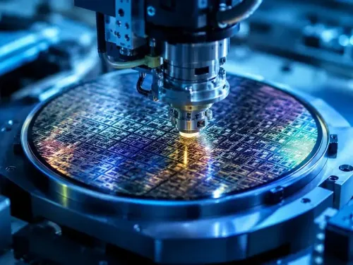
The government has approved 12 semiconductor projects across six states, with investment commitments exceeding ₹1.64 lakh crore. These projects span silicon and compound semiconductor fabrication facilities, display fabrication units, and advanced packaging infrastructure. Crucially, three facilities have already commenced commercial production — marking what officials describe as India's transition from semiconductor policy to actual manufacturing output.
Notably, 211 chips were taped out by 75 institutions by April 2026, demonstrating a measurable expansion in domestic chip design capacity. This is not a marginal figure — it reflects institutional participation from academia, research bodies, and private enterprises working within India's design ecosystem.
Semicon 2.0: Scaling to Global Leadership
Building on this foundation, the government has approved Semicon 2.0 with an outlay of ₹1,27,500 crore in July 2026. The programme is designed to support semiconductor intellectual property (IP), chip and system designs, and to consolidate India's positioning as a global semiconductor design hub.
'Semicon 2.0 will further intend to support semiconductor IP, chip and system designs, strengthening India's position as a global semiconductor design hub. By strengthening domestic capabilities today, India is positioning itself to shape the technologies of tomorrow,' the official statement said.
This comes amid intensifying global competition in chip manufacturing, with the United States, European Union, Japan, and South Korea each committing hundreds of billions of dollars to domestic semiconductor capacity. India's entry — while later — is being structured around design-led manufacturing rather than pure volume fabrication.
IndiaAI Mission: GPUs and Subsidised Compute
Parallel to the semiconductor drive, the IndiaAI Mission — approved with an outlay of approximately ₹10,372 crore — has recorded significant progress. Shared compute capacity has been expanded to more than 45,000 Graphics Processing Units (GPUs) as of June 2026.
By August 2026, 237 projects had accessed subsidised AI computing resources, collectively consuming 93.18 lakh GPU hours. This infrastructure is designed to lower entry barriers for Indian researchers, start-ups, and innovators by providing affordable high-performance computing for AI model development, training, testing, and research.
The Semiconductor-AI Convergence
Officials have explicitly framed semiconductors and artificial intelligence as inseparable technologies. AI is accelerating demand for advanced chips, specialised processors, and high-performance computing infrastructure — and India's strategy reflects this convergence by building capabilities from chip design all the way to indigenous AI model development.
With Semicon 2.0 disbursements expected to scale through 2027 and the IndiaAI Mission expanding compute access, the next 18 months will be a critical test of whether India's semiconductor and AI ambitions translate into globally competitive output.
Point of View
But the harder test lies ahead. Fabricating seven chips and bringing three facilities to commercial production is a genuine milestone — not a policy brochure. Yet India's semiconductor ambitions face a structural challenge: the global chip race is being run by state-backed players with decades of ecosystem depth, and India is building that ecosystem largely from scratch. Semicon 2.0's ₹1,27,500 crore outlay is substantial, but disbursement timelines and yield rates at advanced nodes will matter far more than committed capital. The IndiaAI Mission's 45,000-GPU compute pool is a meaningful intervention for start-ups, but remains a fraction of what frontier AI model training demands. India's bet is on design-led differentiation — a viable niche, but one that requires sustained, decade-long execution discipline that Indian industrial policy has historically struggled to maintain.
NationPress
28 Sept 2026
Frequently Asked Questions
How many semiconductor projects has India approved and what is the total investment?
India has approved 12 semiconductor projects across six states, with investment commitments exceeding ₹1.64 lakh crore. The projects cover silicon and compound semiconductor fabs, display fabrication, and advanced packaging facilities.
What is Semicon 2.0 and when was it approved?
Semicon 2.0 is India's next-phase semiconductor programme approved in July 2026 with an outlay of ₹1,27,500 crore. It is designed to support semiconductor IP, chip and system designs, and to strengthen India's position as a global semiconductor design hub.
What progress has the IndiaAI Mission made?
The IndiaAI Mission, approved with an outlay of approximately ₹10,372 crore, has expanded shared compute capacity to over 45,000 GPUs as of June 2026. By August 2026, 237 projects had accessed 93.18 lakh GPU hours of subsidised AI computing.
Has India actually fabricated chips domestically, and at what technology nodes?
Yes. According to an official government factsheet, seven chips have been successfully fabricated at various process nodes, including advanced nodes such as 12 nm. Additionally, 211 chips were taped out by 75 institutions by April 2026.
Which facilities have started commercial semiconductor production in India?
Three facilities have commenced commercial production as of August 2026, according to the government factsheet. Officials described this as India's transition from semiconductor policy to on-ground manufacturing.