Semicon 2.0: India's ₹1,27,500 crore bet on chip design and R&D

Synopsis
Semicon 2.0 is not just a bigger cheque — it is a fundamentally different bet. With ₹1,27,500 crore committed and a 75 per cent R&D subsidy on offer, India is signalling that it wants to own chips intellectually, not just assemble them. The pivot from capacity to design and IP could be the most consequential industrial policy shift of the decade.
Key Takeaways
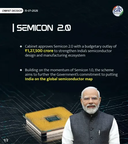
Semicon 2.0 carries a ₹1,27,500 crore outlay, aiming to attract ₹4 lakh crore in investment and enable ₹2 lakh crore of semiconductor production.
The scheme rests on six pillars : chip design, machines and materials, additional fabs, ATMP/OSAT strengthening, R&D, and talent development.
Fiscal incentives include 40% capex support for silicon fabs and up to 75% combined Centre-and-state support for R&D and talent.
The talent pillar targets training of one lakh design engineers within five years.
India aims to capture 10% of the projected $1.8–2 trillion global semiconductor market by 2035 .
ICEA urged states to act fast, warning that first movers will attract entire ecosystems, not just individual plants.
India's Semicon 2.0 scheme, backed by a ₹1,27,500 crore outlay, marks a strategic pivot away from pure manufacturing capacity toward design, research and development, and supply-chain depth across the domestic semiconductor ecosystem, industry experts said on Monday, 31 August. The scheme is designed to attract approximately ₹4 lakh crore in investment and enable roughly ₹2 lakh crore of semiconductor production over its tenure.
Six Pillars of the Scheme
Semicon 2.0 rests on six pillars: chip design; machines and materials; additional fabrication facilities; strengthening of the ATMP/OSAT industry; research and development; and talent development. The talent pillar alone targets training of one lakh design engineers within five years, alongside manufacturing skills spanning fabrication, packaging, equipment, and materials.
On the fiscal side, the scheme offers 40 per cent capex support for silicon fabs on a pari-passu basis, and up to 75 per cent combined Centre-and-state support for R&D and talent initiatives — among the most aggressive incentive structures India has offered the sector.
What Industry Leaders Said
Pankaj Mohindroo, Chairman of the India Cellular and Electronics Association (ICEA), said: 'Building Indian-owned chip-design capability, including for AI compute, will allow companies to move higher up the value chain, retain a larger share of global electronics and generate growth that is recurring and durable not dependent on a single manufacturing cycle.'
Mohindroo added: 'Government's focus on developing domestic design and R&D will pave the way for long-term and sustained growth of the industry. Design is where value, intellectual property and strategic control reside.'
Aisha Ali Hussaini, Partner and Semiconductor Tax Leader at EY India, said the programme is 'aligned with India's ambition to capture 10 per cent of the projected $1.8–2 trillion global semiconductor market by 2035' and provides 'a robust foundation for long-term economic growth by strengthening the domestic semiconductor value chain.'
Paritosh Prajapati, CEO of GX Group, said the scheme's focus on advanced packaging, chip design, displays, and other critical semiconductor technologies will strengthen domestic capabilities across the value chain.
The Push for Indian-Owned IP
The ICEA urged companies, investors, and state governments to act swiftly to convert the policy framework into concrete projects and Indian-owned intellectual property. The association stressed that all components of the ecosystem — design, AI compute, and domestic IP — must advance in tandem with manufacturing and the broader supply chain.
Notably, the ICEA warned that states which move first will lock in a first-mover advantage, attracting not just standalone plants but entire ecosystems comprising fabs, packaging units, suppliers, design houses, and talent pools.
Why This Shift Matters
India's earlier semiconductor push under Semicon India concentrated heavily on attracting fabrication plants. Semicon 2.0 signals a more sophisticated ambition: capturing value at the design and IP layer, where margins and strategic leverage are significantly higher. This comes amid intensifying global competition for semiconductor supply-chain diversification, with the US, EU, Japan, and South Korea all deploying large public subsidies to anchor chip production domestically.
With the global semiconductor market projected to reach $1.8–2 trillion by 2035, India's ability to secure even a fraction of that through design and R&D leadership — rather than low-cost assembly — could reshape its position in the global technology hierarchy.
Point of View
But the execution risk is substantial. India has announced semiconductor ambitions before, and the gap between policy frameworks and operational fabs has historically been wide. The 75 per cent R&D subsidy is aggressive, but subsidies alone do not produce design talent or IP — that requires universities, startups, and a risk-tolerant private sector working in concert. The one-lakh-engineer target sounds large; without a credible pipeline from engineering colleges to design houses, it risks becoming another headline number. The ICEA's first-mover framing for states is strategically sound, but without a central implementation body with real teeth, the scheme could fragment into 28 different state-level experiments.
NationPress
16 Oct 2026
Frequently Asked Questions
What is India's Semicon 2.0 scheme?
Semicon 2.0 is the Indian government's updated semiconductor policy, backed by a ₹1,27,500 crore outlay, designed to shift focus from building manufacturing capacity to developing chip design, R&D, and supply-chain capabilities. It aims to attract ₹4 lakh crore in investment and enable ₹2 lakh crore of semiconductor production over the scheme period.
What are the six pillars of Semicon 2.0?
The scheme rests on six pillars: chip design; machines and materials; additional fabrication facilities; strengthening of the ATMP/OSAT industry; research and development; and talent development. The talent pillar targets training one lakh design engineers within five years.
What fiscal incentives does Semicon 2.0 offer?
The scheme offers 40 per cent capex support for silicon fabs on a pari-passu basis, and up to 75 per cent combined Centre-and-state support for R&D and talent initiatives — among the most generous incentive structures India has offered the semiconductor sector.
What is India's semiconductor market target by 2035?
India aims to capture 10 per cent of the projected $1.8–2 trillion global semiconductor market by 2035, according to EY India's Semiconductor Tax Leader Aisha Ali Hussaini. Semicon 2.0 is positioned as the primary policy vehicle to achieve that ambition.
Why is the focus on design and R&D rather than manufacturing?
Design and R&D are where the highest margins, intellectual property, and strategic control in the semiconductor value chain reside, according to ICEA Chairman Pankaj Mohindroo. By building Indian-owned chip-design capability, companies can move higher up the value chain and generate growth that is recurring and not dependent on a single manufacturing cycle.