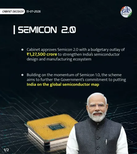
Semicon 2.0: India's ₹1.27 lakh crore chip push to create 2 lakh jobs by 2030
Synopsis
India's Semicon 2.0 isn't just another industrial scheme — it's a structural pivot. With ₹1.27 lakh crore committed, 12 projects already approved, and a mandate to move from assembly to chip design and fabrication, the programme targets up to 2 lakh jobs by 2030 and a seat at the global semiconductor table during a once-in-a-generation supply chain realignment.
Key Takeaways
Semicon 2.0 , approved by the Union Cabinet , carries a budget outlay of ₹1.27 lakh crore .
The scheme is projected to create 1.5 lakh–2 lakh direct and indirect jobs over the next five years .
Nearly 70 per cent of semiconductor and electronics roles are expected to evolve by 2030 , according to NLB Services .
Semiconductor-focused GCCs are projected to grow by 25–30 per cent by 2030.
The government has already approved 12 semiconductor manufacturing projects with cumulative investments exceeding ₹1.64 lakh crore .
Phase 1 secured more than $20 billion in announced semiconductor projects, according to IESA .
India's Semicon 2.0 scheme is projected to generate between 1.5 lakh and 2 lakh direct and indirect jobs over the next five years, while fundamentally reshaping the country's electronics sector from an assembly-driven base into a globally competitive hub for chip design, engineering, and innovation, according to industry analysis released on Friday, 17 July 2025.
What Semicon 2.0 Covers
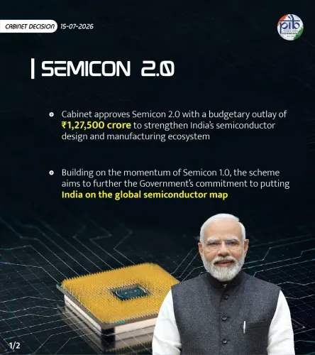
The Union Cabinet, chaired by Prime Minister Narendra Modi, recently approved the Semicon 2.0 scheme with a budget outlay of ₹1.27 lakh crore. The programme is structured around six key pillars: chip design, semiconductor manufacturing equipment and materials, fabrication facilities, ATMP/OSAT units, research and development, and talent development.
According to analysis by NLB Services, this next phase moves decisively beyond assembly manufacturing to build an integrated ecosystem spanning chip design, semiconductor verification, embedded systems, electronic design automation (EDA), AI-enabled manufacturing, advanced packaging, and intelligent supply chain operations.
Jobs and Talent Outlook
Sachin Alug, Chief Executive Officer of NLB Services, said nearly 70 per cent of roles across the semiconductor and electronics ecosystem are expected to evolve by 2030, generating strong demand for high-skilled engineering talent. He also projected a 25–30 per cent increase in semiconductor-focused Global Capability Centres (GCCs) by 2030, further consolidating India's standing as a global engineering, research, and innovation destination.
Alug noted that while India's electronics manufacturing has historically been dominated by assembly operations, Semicon 2.0 offers a concrete pathway to move up the value chain through capabilities in chip design, fabrication, testing, and advanced packaging — areas that generate higher-value intellectual property and long-term competitive advantage.
Building on Phase 1 Momentum
The India Electronics and Semiconductor Association (IESA) had earlier noted that Phase 1 of the semiconductor mission had already helped secure more than $20 billion in announced semiconductor projects. Phase 2's expanded emphasis on fabs, advanced packaging, design, R&D, talent, equipment, and materials aims to position India as a trusted global semiconductor partner.
So far, the government has approved 12 semiconductor manufacturing projects with cumulative investments exceeding ₹1.64 lakh crore — a figure that underscores the scale of private and public capital now committed to the sector.
Why This Matters for India's Industrial Future
This comes amid a global scramble to diversify semiconductor supply chains away from East Asia, with the United States, European Union, and Japan each running parallel incentive programmes. India's Semicon 2.0 positions the country to capture a share of that realignment. Notably, the scheme's focus on design and R&D — rather than fabrication alone — reflects a strategic bet that India's engineering talent pool is its most durable competitive asset.
With guidelines now in place and investments already committed, the sector's next milestone will be translating announced projects into operational capacity and verifiable job creation on the ground.
Point of View
But the real test lies in execution — specifically, whether India can build genuine fabrication and design capacity or remain a high-end assembly destination with better branding. The 70 per cent role-evolution figure from NLB Services signals a talent demand that India's engineering colleges are not yet calibrated to meet at scale. Meanwhile, the $20 billion secured under Phase 1 in announcements has yet to fully translate into operational fabs. The scheme's six-pillar structure is architecturally sound, but without independent tracking of job creation and IP generation, it risks becoming another well-designed programme measured by investment commitments rather than industrial outcomes.
NationPress
15 Oct 2026
Frequently Asked Questions
What is India's Semicon 2.0 scheme?
Semicon 2.0 is a government programme approved by the Union Cabinet with a budget outlay of ₹1.27 lakh crore, aimed at building India's semiconductor design and manufacturing ecosystem across six pillars including chip design, fabrication, ATMP/OSAT units, R&D, and talent development. It is the second phase of India's semiconductor mission and expands significantly on Phase 1.
How many jobs will Semicon 2.0 create?
Industry analysis by NLB Services projects that Semicon 2.0 will create between 1.5 lakh and 2 lakh direct and indirect jobs over the next five years. Nearly 70 per cent of roles in the semiconductor and electronics ecosystem are expected to evolve by 2030, driving demand for high-skilled engineering talent.
What did Phase 1 of India's semiconductor mission achieve?
According to IESA, Phase 1 helped secure more than $20 billion in announced semiconductor projects. The government has so far approved 12 semiconductor manufacturing projects with cumulative investments exceeding ₹1.64 lakh crore.
How will Semicon 2.0 change India's electronics industry?
The scheme aims to shift India's electronics sector from an assembly-led model to a globally competitive hub for chip design, fabrication, testing, and advanced packaging. This move up the value chain is expected to generate higher-value intellectual property and long-term competitive advantage for Indian industry.
What is the outlook for semiconductor GCCs in India?
NLB Services CEO Sachin Alug projects a 25–30 per cent increase in semiconductor-focused Global Capability Centres (GCCs) in India by 2030, reinforcing the country's position as a global engineering, research, and innovation hub.