Cabinet Clears Semicon 2.0 With Rs 1.27 Lakh Crore Outlay
Synopsis
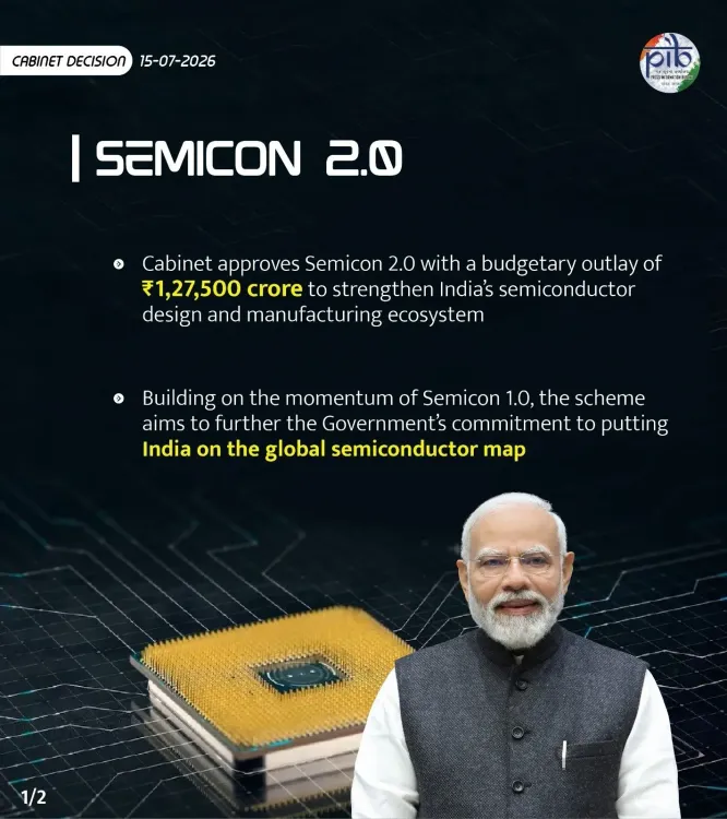
The Union Cabinet on 15 July 2026 approved Semicon 2.0 with a Rs 1,27,500 crore outlay, expanding India's semiconductor mission across six pillars — chip design, fabs, OSAT, machinery, R&D and talent — to make India a global semiconductor hub by 2047.
Key Takeaways
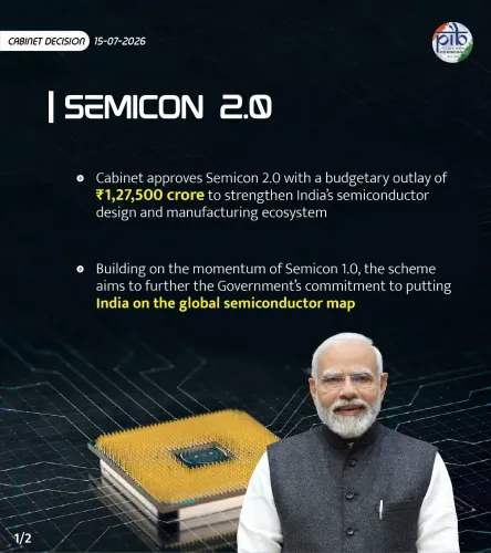
The Union Cabinet chaired by Prime Minister Narendra Modi approved Semicon 2.0 on 15 July 2026 .
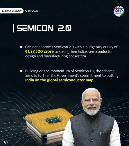
The mission carries a total budget outlay of Rs 1,27,500 crore , more than doubling the Rs 76,000 crore committed under Semicon 1.0 in 2021.
Six pillars anchor the mission: chip design, semiconductor machinery and materials, fabrication units, advanced ATMP/OSAT facilities, R&D, and talent development.
The scheme aims to generate high-skilled employment , attract foreign and domestic investment, and strengthen India's supply-chain resilience.
Semicon 2.0 is aligned with the government's Viksit Bharat 2047 vision of a fully developed Indian economy by the centenary of independence.
MeitY is expected to issue project-wise allocations and the first fab or OSAT approvals in the months ahead.
The Union Cabinet, chaired by Prime Minister Narendra Modi, approved Semicon 2.0 on Wednesday, 15 July 2026 — a comprehensive mission to develop India's semiconductor design and manufacturing ecosystem with a total budget outlay of Rs 1,27,500 crore. Union Health Minister and BJP national president J. P. Nadda announced the decision, describing it as a landmark step toward positioning India as a global semiconductor hub.
Context
Semicon 2.0 builds directly on the original India Semiconductor Mission (Semicon 1.0), which the Union Cabinet approved in December 2021 with an outlay of Rs 76,000 crore. That earlier programme was designed to attract semiconductor investments by offering fiscal incentives for fabrication plants and assembly, testing, marking and packaging (ATMP) facilities. The new mission more than doubles the financial commitment, signalling a significant escalation in ambition and urgency.
The approved scheme is structured around six key pillars: chip design, semiconductor machinery and materials, fabrication units (fabs), advanced ATMP and outsourced semiconductor assembly and test (OSAT) facilities, research and development, and talent development. Nadda's post on X described the mission as one that will 'boost innovation, attract investments, generate high-skilled employment, strengthen supply chain resilience, enhance technological self-reliance, and accelerate the journey towards Viksit Bharat 2047.'
Policy Backdrop
India's semiconductor push is rooted in the Atmanirbhar Bharat programme and the broader Production Linked Incentive (PLI) framework launched in 2020, which sought to reduce import dependence across critical sectors following pandemic-era supply-chain disruptions. Geopolitical concentration of chip manufacturing in Taiwan and China added strategic urgency to building domestic capacity.
The effort gained an international dimension in 2023 when India and the United States formalised cooperation on critical and emerging technologies, with semiconductors identified as a priority sector. Under Semicon 1.0, the government issued initial approvals for fabrication and assembly projects, laying the groundwork that Semicon 2.0 now seeks to scale. The Ministry of Electronics and Information Technology (MeitY) is expected to issue project-wise allocation details in the coming months.
Stakeholders and Impact
The mission is expected to benefit a wide ecosystem: domestic and multinational semiconductor firms seeking a cost-competitive manufacturing base, electronics manufacturers looking to shorten supply chains, and engineering graduates who stand to gain from the talent-development pillar. High-skilled employment generation is explicitly cited as a goal, making the scheme relevant to India's large pool of science and technology graduates.
Analysts note that successful fab and OSAT capacity would reduce India's dependence on imported chips — a vulnerability exposed during the 2021-22 global chip shortage that disrupted automotive and consumer electronics production. A robust domestic semiconductor ecosystem would also support sectors such as defence electronics, telecommunications, and electric vehicles that are central to India's industrial roadmap.
What's Next
Attention will now turn to MeitY notifications detailing project-wise allocations and the first set of fab or OSAT approvals expected in subsequent months. Industry observers will watch whether the enhanced outlay translates into confirmed investments from global chipmakers and whether the talent-development pillar produces a credible pipeline of semiconductor engineers. Progress on Semicon 2.0 will be a key indicator of how seriously India is closing the gap with established semiconductor nations ahead of Viksit Bharat 2047.
Point of View
More than doubling the original semiconductor mission outlay in under five years. The six-pillar architecture — spanning design, materials, fabs, packaging, R&D and talent — signals a shift from incentivising individual projects to building an end-to-end domestic ecosystem. Politically, the announcement reinforces the 'Atmanirbhar Bharat' narrative ahead of a period when global chip supply chains remain fragile and strategically contested. The real test will be execution: whether India can attract credible fab investments and produce semiconductor engineers at scale before rival economies consolidate their own positions.
NationPress
14 Oct 2026
Frequently Asked Questions
What is Semicon 2.0 approved by the Indian Cabinet?
Semicon 2.0 is a Union Cabinet-approved mission to develop India's semiconductor design and manufacturing ecosystem, with a total outlay of Rs 1,27,500 crore. It covers six pillars: chip design, semiconductor machinery and materials, fabrication units, ATMP/OSAT facilities, R&D, and talent development.
What is the budget of India's Semicon 2.0 mission?
The approved budget outlay for Semicon 2.0 is Rs 1,27,500 crore, announced on 15 July 2026 by the Union Cabinet chaired by Prime Minister Narendra Modi.
How is Semicon 2.0 different from Semicon 1.0?
Semicon 1.0, approved in December 2021, had an outlay of Rs 76,000 crore and focused on attracting initial semiconductor investments. Semicon 2.0 more than doubles the financial commitment and adds a structured six-pillar framework including R&D and talent development.
What is the goal of India's semiconductor mission?
The mission aims to position India as a global semiconductor hub by boosting chip design and manufacturing, attracting investment, generating high-skilled jobs, and reducing import dependence — all in support of the Viksit Bharat 2047 vision.
Who announced Semicon 2.0 Cabinet approval?
Union Health Minister and BJP national president J. P. Nadda announced the Cabinet approval of Semicon 2.0 on X on 15 July 2026, following the Cabinet meeting chaired by Prime Minister Narendra Modi.