Cabinet Clears Semicon 2.0 With ₹1,27,500 Cr Outlay: Shekhawat
Synopsis
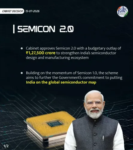
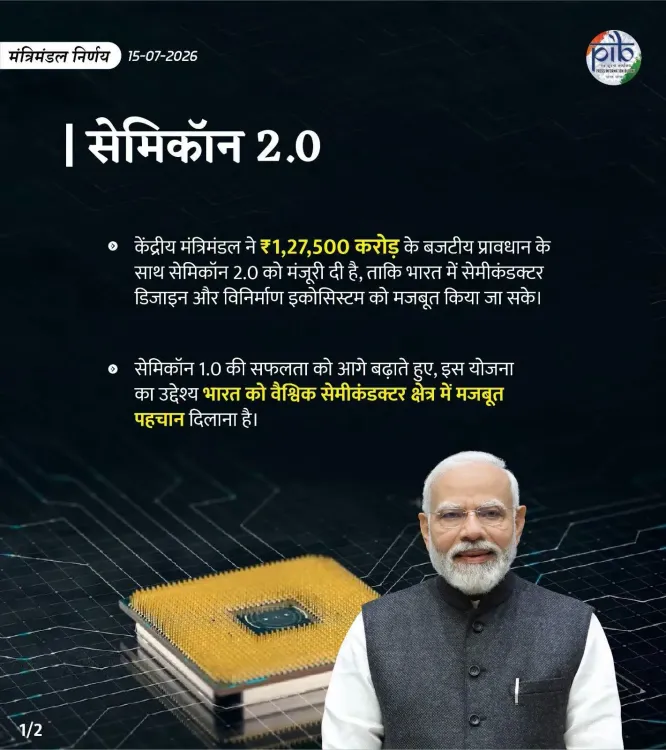
The Union Cabinet on 15 July 2026 approved Semicon 2.0 with a ₹1,27,500 crore outlay, a major expansion of India's 2021 semiconductor scheme. Culture Minister Gajendra Singh Shekhawat called it a defining decision for India's chip manufacturing ambitions under the Modi government.
Key Takeaways
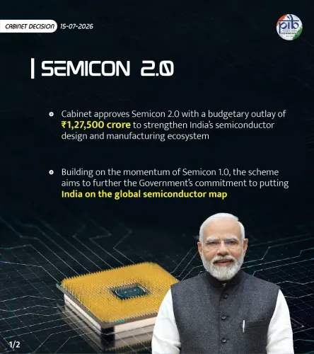
The Union Cabinet approved Semicon 2.0 on 15 July 2026 with a total outlay of ₹1,27,500 crore .
The new outlay is approximately 68 per cent higher than the original ₹76,000 crore Semicon India Programme approved in December 2021 .
The scheme aims to build a domestic semiconductor and display manufacturing ecosystem under the Atmanirbhar Bharat framework.
The India Semiconductor Mission (ISM) under MeitY is the nodal agency responsible for implementing semiconductor policy and attracting fabrication investments.
The approval is expected to benefit the electronics, automotive, defence, and telecom sectors through improved domestic chip availability.
Union Minister Gajendra Singh Shekhawat described the decision as giving 'a new dimension' to India's semiconductor sector.
Union Culture and Tourism Minister Gajendra Singh Shekhawat on Wednesday, 15 July 2026, hailed the Union Cabinet's approval of Semicon 2.0 — a revised and significantly expanded semiconductor manufacturing initiative — calling it a landmark decision that will give India's semiconductor sector a new dimension. The Cabinet cleared the scheme with a total outlay of ₹1,27,500 crore.
Context
Shekhawat posted on X, writing in Hindi: '₹1,27,500 करोड़ के परिव्यय के साथ सेमिकॉन 2.0 को मोदी सरकार के मंत्रिमंडल द्वारा स्वीकृति भारत के सेमीकंडक्टर क्षेत्र को नया आयाम देने वाला महत्वपूर्ण निर्णय है' — translating to: 'The Cabinet's approval of Semicon 2.0 with an outlay of ₹1,27,500 crore is an important decision that will give a new dimension to India's semiconductor sector.' The post carried the hashtag #CabinetDecisions, signalling coordinated BJP communication around the Cabinet meeting's outcomes.
The Union Cabinet, chaired by Prime Minister Narendra Modi, is the apex decision-making body of the Indian government. Approvals of this scale require Cabinet sanction and are typically implemented through nodal ministries.
Policy Backdrop
India's semiconductor push has a clear lineage. In December 2021, the Union Cabinet approved the original Semicon India Programme with an outlay of ₹76,000 crore, aimed at building a domestic semiconductor and display manufacturing ecosystem through fiscal incentives and infrastructure support. The India Semiconductor Mission (ISM), set up under the Ministry of Electronics and Information Technology (MeitY), was designated the nodal agency for implementation.
Semicon 2.0 represents a substantial scaling-up of that original commitment — the new outlay of ₹1,27,500 crore is roughly 68 per cent higher than the 2021 allocation. The expansion fits within the broader Atmanirbhar Bharat framework launched in 2020, which set explicit targets for domestic chip production and reducing dependence on imports from Taiwan and China.
Geopolitical tailwinds have reinforced the urgency. Global chip shortages exposed supply-chain vulnerabilities, and frameworks such as the US-India initiative on Critical and Emerging Technology (iCET) have positioned semiconductor collaboration as a strategic priority between New Delhi and Washington.
Stakeholders and Impact
The primary beneficiaries of Semicon 2.0 are expected to be domestic and international semiconductor manufacturers and the wider electronics industry that depends on reliable chip supply. Successive Production-Linked Incentive (PLI) schemes for electronics have already attracted interest from companies exploring wafer fabrication and chip assembly investments in India.
For the broader economy, a robust domestic semiconductor base would reduce the import bill for chips — one of India's largest import categories — and create high-skill manufacturing employment. Consumer electronics, automotive, defence, and telecom sectors all stand to benefit from improved chip availability and pricing stability.
What's Next
The Cabinet approval is the policy trigger; execution now moves to MeitY and the India Semiconductor Mission, which will be expected to operationalise project approvals, disburse incentives, and attract foreign direct investment under the updated scheme. Analysts and industry watchers will track whether major fabrication investments — including from domestic conglomerates and international foundries — are announced in the near term under Semicon 2.0's enhanced financial envelope. India's ambition to become a credible node in the global semiconductor supply chain will be tested by the pace and scale of those project commitments.
Frequently Asked Questions
What is Semicon 2.0 India?
Semicon 2.0 is an updated and expanded version of India's original Semicon India Programme, approved by the Union Cabinet on 15 July 2026 with an outlay of ₹1,27,500 crore to promote domestic semiconductor and display manufacturing.
How much money has India allocated for semiconductor manufacturing under Semicon 2.0?
The Union Cabinet approved an outlay of ₹1,27,500 crore for Semicon 2.0, significantly higher than the ₹76,000 crore allocated under the original 2021 Semicon India Programme.
Who implements India's semiconductor policy?
The India Semiconductor Mission (ISM), a nodal agency set up under the Ministry of Electronics and Information Technology (MeitY), is responsible for implementing semiconductor policy and attracting investments for fabrication units.
Why is India investing heavily in semiconductor manufacturing?
India is investing in semiconductors to reduce dependence on chip imports from Taiwan and China, strengthen supply-chain resilience, create high-skill jobs, and position itself as a node in the global semiconductor supply chain under the Atmanirbhar Bharat initiative.
What did Gajendra Singh Shekhawat say about Semicon 2.0?
Union Culture and Tourism Minister Gajendra Singh Shekhawat posted on X that the Cabinet's approval of Semicon 2.0 with a ₹1,27,500 crore outlay is 'an important decision that will give a new dimension to India's semiconductor sector.'