Cabinet Clears Semicon 2.0 With Rs 1,27,500 Cr Outlay
Synopsis
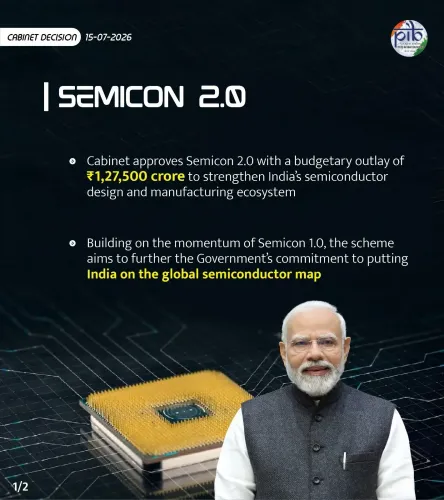
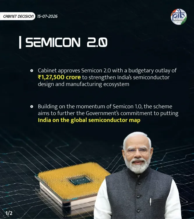
The Union Cabinet under PM Modi has approved Semicon 2.0 with a Rs 1,27,500 crore budgetary provision, targeting chip design, new fabs, ATMP/OSAT, R&D and talent development to place India firmly on the global semiconductor map.
Key Takeaways
The Union Cabinet approved Semicon 2.0 on 15 July 2026 under PM Narendra Modi's leadership.
The programme carries a budgetary provision of Rs 1,27,500 crore — up from the Rs 76,000 crore committed under the original India Semiconductor Mission in 2021.
Key focus areas include chip design , semiconductor equipment and materials manufacturing , new fab establishment , and ATMP/OSAT industry strengthening .
R&D and talent development are embedded as core pillars of the programme, not peripheral components.
The initiative is framed as central to achieving Viksit Bharat and reducing India's dependence on semiconductor imports from East Asia .
Subsequent project-level approvals and disbursement timelines will determine the actual implementation pace.
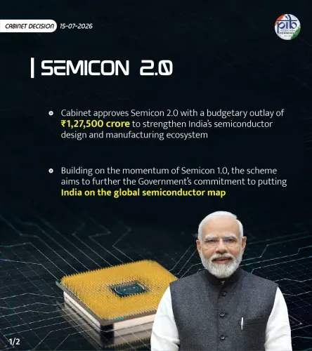
Union Agriculture Minister Shivraj Singh Chouhan announced on Wednesday, 15 July 2026 that the Union Cabinet, under the leadership of Prime Minister Narendra Modi, has approved 'Semicon 2.0' — a landmark programme carrying a budgetary provision of Rs 1,27,500 crore — to strengthen India's semiconductor design and manufacturing ecosystem.
Sharing the cabinet decision on X, Chouhan wrote that Semicon 2.0 would place special emphasis on chip design, semiconductor equipment and material manufacturing, new fab establishment, ATMP/OSAT industry strengthening, research and development, and talent development — covering nearly every link in the semiconductor value chain.
Context
The cabinet's approval marks a significant escalation of India's semiconductor ambitions. The government's earlier India Semiconductor Mission, approved in 2021 with an outlay of Rs 76,000 crore, provided the foundational incentive framework that attracted the first wave of fab investments. Semicon 2.0, at Rs 1,27,500 crore, represents a roughly 68 per cent increase in committed public resources, signalling that New Delhi views semiconductor self-reliance as a long-term strategic priority rather than a one-time push.
India's drive for domestic chip capacity sits within the broader Atmanirbhar Bharat framework, which since 2020 has sought to reduce the country's dependence on semiconductor imports concentrated in East Asia. Global supply-chain disruptions — most acutely felt during the 2021–22 chip shortage — underscored the strategic risk of that dependence and accelerated policy action in New Delhi.
Policy Backdrop
The India Semiconductor Mission catalysed project-level commitments from firms including Tata Electronics and Micron Technology, with several state governments offering complementary land and infrastructure incentives. Semicon 2.0 builds on that foundation by explicitly targeting upstream segments — equipment and materials manufacturing — that were less addressed in the first phase, and by embedding R&D and talent development as core pillars rather than ancillary components.
The inclusion of ATMP (Advanced Test, Marking and Packaging) and OSAT (Outsourced Semiconductor Assembly and Test) support is notable: these back-end operations are where much of the value-addition in chip manufacturing occurs and where India has historically had very limited capacity. Strengthening this segment could allow Indian facilities to serve as packaging and testing hubs for global chip designers even before full-scale fabrication matures.
Stakeholders and Impact
The programme's beneficiaries span a wide arc — from large semiconductor fabrication firms and electronics manufacturers seeking supply-chain certainty, to engineering graduates and technical workforce who stand to gain from the talent development component. Domestic electronics brands reliant on imported chips could see improved input security over the medium term.
Chouhan noted in his post that the initiative would play an important role in placing India firmly on the 'vaishvik semiconductor manchitra' (global semiconductor map), strengthening supply chains, accelerating economic growth, establishing technological leadership, and realising the vision of a Viksit Bharat (Developed India). For the broader technology sector, the policy sends a clear signal that New Delhi intends to compete with established semiconductor hubs in Taiwan, South Korea, and increasingly the United States and Europe.
What's Next
Implementation pace will be determined by subsequent project-level approvals, disbursement timelines, and any new international technology-transfer or co-investment partnerships that the government announces. The Ministry of Electronics and Information Technology, which administers the India Semiconductor Mission, is expected to issue detailed guidelines for Semicon 2.0 applications. Analysts will watch whether the expanded outlay translates into new fab groundbreakings or remains at the incentive-framework stage in the near term.
With Rs 1,27,500 crore now formally committed, India's semiconductor policy has entered a new phase — one that tests whether fiscal ambition can be converted into installed wafer capacity and a self-sustaining domestic chip industry.
Point of View
The gap between announced outlays and actual disbursements has historically been a weak point in India's industrial policy, and the semiconductor sector's technical barriers are uniquely high. The political optics of the announcement — shared by the Agriculture Minister rather than the Electronics Minister — also suggest the cabinet is treating this as a whole-of-government milestone, reinforcing the Viksit Bharat narrative ahead of upcoming electoral cycles.
NationPress
14 Oct 2026
Frequently Asked Questions
What is Semicon 2.0 India?
Semicon 2.0 is a Union Cabinet-approved programme with a budgetary provision of Rs 1,27,500 crore aimed at strengthening India's semiconductor design, fabrication, packaging, testing, R&D and talent ecosystem.
How much money has India allocated for Semicon 2.0?
The Union Cabinet has approved a budgetary provision of Rs 1,27,500 crore for Semicon 2.0, announced on 15 July 2026.
What is the difference between India Semiconductor Mission and Semicon 2.0?
The original India Semiconductor Mission, approved in 2021, had an outlay of Rs 76,000 crore focused on incentivising fab and assembly units. Semicon 2.0 expands the commitment to Rs 1,27,500 crore and adds explicit pillars for equipment manufacturing, ATMP/OSAT, R&D and talent development.
What is ATMP and OSAT in the context of Indian semiconductors?
ATMP stands for Advanced Test, Marking and Packaging, while OSAT means Outsourced Semiconductor Assembly and Test — both refer to back-end chip manufacturing processes where India has historically had limited capacity and which Semicon 2.0 aims to develop.
Who announced Semicon 2.0 cabinet approval?
Union Agriculture Minister Shivraj Singh Chouhan announced the cabinet approval of Semicon 2.0 on X on 15 July 2026, attributing the decision to PM Narendra Modi's leadership.