Amit Shah hails Semicon 2.0 outlay of ₹1.27 lakh crore
Synopsis
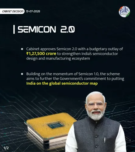
The Union Cabinet has approved Semicon 2.0 with a ₹1.27 lakh crore outlay to build India's semiconductor ecosystem across six strategic pillars. Union Home Minister Amit Shah called it a giant step toward making India a global chip powerhouse, scaling up the 2021 India Semiconductor Mission under PM Modi's Atmanirbhar Bharat vision.
Key Takeaways
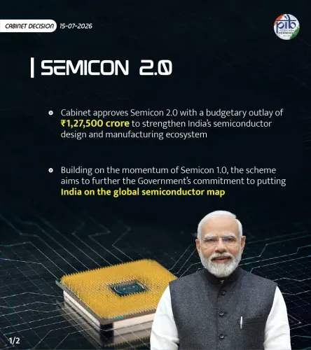
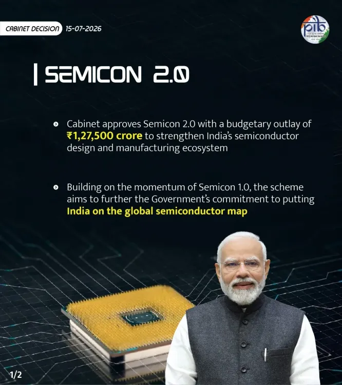
The Union Cabinet approved Semicon 2.0 on 15 July 2026 with a total outlay of ₹1.27 lakh crore .
Union Home Minister Amit Shah described the move as 'a giant step towards turning India into a semiconductor titan.' The initiative targets six strategic pillars of the semiconductor ecosystem, including talent development.
Semicon 2.0 builds on the original ₹76,000 crore semiconductor and display manufacturing scheme approved in 2021 that created the India Semiconductor Mission .
The programme aims to reduce India's chip import dependence on Taiwan , South Korea , and China .
Cabinet-notified guidelines, state site selections, and new MoUs with global chipmakers are the immediate milestones to watch.
Union Home Minister Amit Shah on Wednesday, 15 July 2026, welcomed the Union Cabinet's approval of Semicon 2.0, a semiconductor initiative backed by an outlay of ₹1.27 lakh crore, calling it a decisive move toward establishing India as a global semiconductor powerhouse as envisioned by Prime Minister Narendra Modi.
Context
Posting on X, Shah described the Cabinet approval as 'a giant step towards turning India into a semiconductor titan.' He added that the initiative would 'nurture talent and develop the six strategic pillars of the semiconductor ecosystem,' positioning India as a nation 'the world looks up to.' The post underscores the political weight the ruling dispensation is placing on semiconductor self-reliance as a flagship technology goal.
The announcement builds on years of policy groundwork. In 2021, the Union Cabinet had approved a ₹76,000 crore semiconductor and display manufacturing scheme that gave birth to the India Semiconductor Mission (ISM), the nodal agency for chip-related investments. Semicon 2.0 represents a significant scaling-up of that original commitment, nearly doubling the financial firepower directed at the sector.
Policy Backdrop
India's semiconductor push is rooted in the broader Atmanirbhar Bharat vision championed by Prime Minister Modi, which seeks to reduce the country's deep dependence on chip imports from Taiwan, South Korea, and China. The India Semiconductor Mission has served as the central coordinating body, offering production-linked incentives, fiscal support for fabrication units, and skilling programmes designed to build a domestic talent pipeline.
The reference to 'six strategic pillars' in Shah's post points to a structured framework likely spanning chip design, wafer fabrication, advanced packaging, compound semiconductors, equipment manufacturing, and human-resource development — though the Cabinet-notified guidelines are expected to detail the precise architecture. State governments have also been active participants, competing to host upcoming fabrication facilities by offering land and infrastructure incentives.
Stakeholders and Impact
The ₹1.27 lakh crore outlay is expected to have cascading effects across the electronics manufacturing value chain, benefiting semiconductor design houses, foundries, assembly and test firms, and the broader consumer electronics sector that relies on domestically sourced chips. Engineering colleges and skilling institutions are also direct stakeholders, given the programme's explicit focus on talent development.
Global chipmakers and foundries that have been in dialogue with New Delhi over potential India-based facilities are likely to view the enhanced outlay as a stronger signal of long-term policy commitment. The scale of fiscal support is intended to close the cost-competitiveness gap that has historically made India a less attractive destination for capital-intensive fabrication investments compared with established hubs in East Asia.
What's Next
Attention will now turn to the Cabinet-notified operational guidelines for Semicon 2.0, the selection of states and sites for new fabrication units, and any fresh memoranda of understanding with international chipmakers. Analysts will also watch whether the programme's skilling component translates into measurable enrolments at engineering and vocational institutions within the first year of implementation.
If executed at the scale envisioned, Semicon 2.0 could mark a structural turning point in India's technology manufacturing story — shifting the country from a net importer of chips to a meaningful node in the global semiconductor supply chain by the early 2030s.
Point of View
Senior ministers are reinforcing a narrative of technological nationalism that has proven electorally resonant. The real test, however, will be execution — translating a large fiscal outlay into operational fabs and a skilled workforce within a competitive global timeline.
NationPress
14 Oct 2026
Frequently Asked Questions
What is Semicon 2.0 approved by the Union Cabinet?
Semicon 2.0 is a central government semiconductor initiative approved by the Union Cabinet with an outlay of ₹1.27 lakh crore, aimed at building India's chip design, fabrication, packaging, and skilling capabilities across six strategic pillars.
What is the outlay for India's new semiconductor scheme in 2026?
The Union Cabinet approved ₹1.27 lakh crore for Semicon 2.0, significantly scaling up the original ₹76,000 crore semiconductor and display manufacturing scheme approved in 2021.
What is the India Semiconductor Mission?
The India Semiconductor Mission (ISM) is the nodal government agency set up after the 2021 Cabinet approval to coordinate chip-related investments, offer production-linked incentives, and attract global foundries and design houses to India.
Why is India investing heavily in semiconductor manufacturing?
India imports a large share of its chips from Taiwan, South Korea, and China. The government's Atmanirbhar Bharat policy seeks to build domestic manufacturing capacity to reduce this dependence and capture a share of the global chip supply chain.
What are the six strategic pillars of India's semiconductor ecosystem?
Union Home Minister Amit Shah's post references six strategic pillars without detailing each one; Cabinet-notified guidelines for Semicon 2.0 are expected to specify the framework, which is broadly understood to cover chip design, fabrication, packaging, compound semiconductors, equipment, and talent development.