Gadkari: Cabinet clears Semicon 2.0 with ₹1.27 lakh cr outlay
Synopsis
The Union Cabinet has approved Semicon 2.0 with a ₹1,27,500 crore budgetary outlay, expanding India's semiconductor mission across six pillars — design, materials, fabrication, ATMP/OSAT, R&D, and talent — to build a globally competitive chip ecosystem.
Key Takeaways
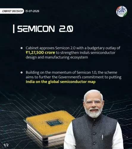
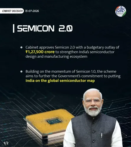
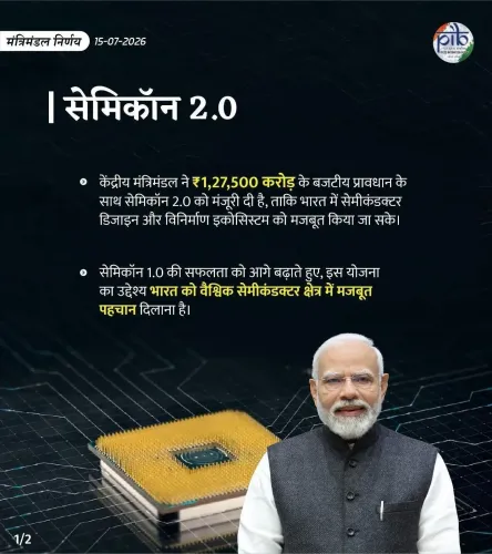
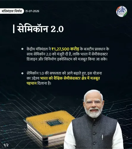
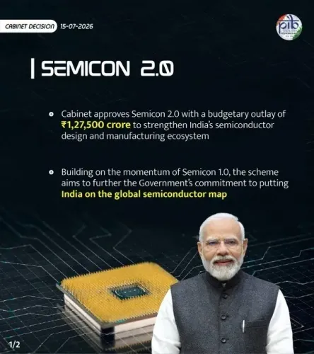
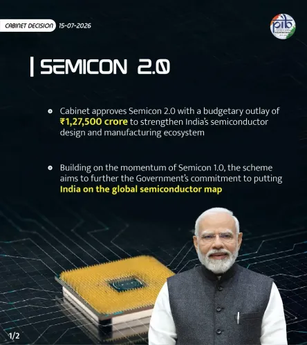
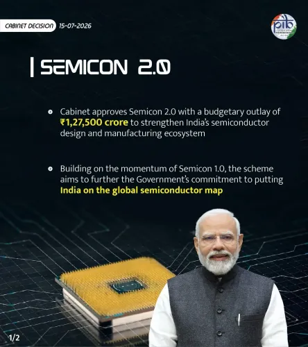
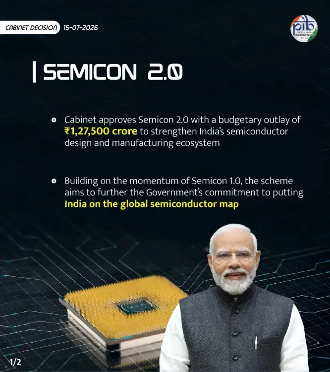
The Union Cabinet , chaired by PM Narendra Modi , approved Semicon 2.0 on 15 July 2026 with a budgetary outlay of ₹1,27,500 crore .
The initiative builds on Semicon 1.0 , which was launched in December 2021 with an outlay of ₹76,000 crore .
Semicon 2.0 is structured around six pillars : design, machines and materials, additional fabs, ATMP/OSAT, R&D, and talent development.
The expanded outlay represents a 67.8% increase over the first phase, reflecting a broader and more ambitious policy scope.
The initiative targets end-to-end semiconductor capability, from chip design to final packaging, to reduce India's import dependence.
Talent development is an explicit pillar, acknowledging human capital as a structural constraint alongside capital investment.
Union Road Transport and Highways Minister Nitin Gadkari on Wednesday, 15 July 2026, announced that the Union Cabinet, chaired by Prime Minister Narendra Modi, has approved Semicon 2.0 — a comprehensive semiconductor development initiative carrying a total budgetary outlay of ₹1,27,500 crore — aimed at accelerating India's semiconductor design and manufacturing ecosystem.
Context
In his post on X, Gadkari described Semicon 2.0 as building on the progress of Semicon 1.0 and reaffirming the government's commitment to positioning India as a global semiconductor hub. The initiative is structured around six key pillars: semiconductor design, machines and materials, establishment of additional fabrication units (fabs), strengthening the ATMP/OSAT (Assembly, Testing, Marking and Packaging / Outsourced Semiconductor Assembly and Test) industry, research and development, and talent development.
Policy Backdrop
India's semiconductor push has its roots in a December 2021 Union Cabinet decision that approved the India Semiconductor Mission with an outlay of ₹76,000 crore. That first phase — now referred to as Semicon 1.0 — focused on attracting investment in fabrication units, chip assembly, and design through production-linked incentives and fiscal support. The Ministry of Electronics and Information Technology has served as the nodal body coordinating policy, incentives, and project approvals under the mission framework.
The jump from ₹76,000 crore to ₹1,27,500 crore in the new phase represents a significant scaling of ambition, reflecting both lessons learnt from the first phase and a sharper focus on end-to-end domestic capability — from chip design through to final packaging and testing. The six-pillar structure signals an intent to address gaps across the entire value chain rather than concentrating support on a single segment.
Stakeholders and Impact
The semiconductor industry — spanning global chip manufacturers, domestic electronics firms, and equipment suppliers — stands to benefit from the expanded fiscal envelope. The explicit inclusion of machines and materials as a dedicated pillar is notable, as this segment has historically been dominated by a handful of countries and represents a critical vulnerability in global supply chains. India has sought to reduce its dependence on semiconductor imports, which feed into everything from consumer electronics to automotive and defence systems.
The talent development pillar directly targets engineering graduates and the broader technical workforce, signalling that the government views human capital as a structural constraint alongside capital investment. Design-linked incentives, if extended under Semicon 2.0, could also energise India's existing base of chip-design firms and fabless startups, many of which operate out of Bengaluru, Hyderabad, and Pune.
What's Next
Attention will now turn to the rollout of specific project approvals — particularly new fabrication units and ATMP facilities — under the expanded outlay. Announcements on design-linked incentive schemes and skill development programmes tied to the six-pillar framework are expected to follow as the Ministry of Electronics and Information Technology operationalises the cabinet decision. The pace at which anchor projects are commissioned will be the key metric by which Semicon 2.0's early progress is judged.
Point of View
Equipment, and human capital that could otherwise constrain downstream manufacturing. Announcing the decision through a senior Cabinet minister's social media post — rather than a dedicated MeitY briefing — also reflects the government's practice of using high-profile political figures to amplify technology policy as part of a broader 'Viksit Bharat' narrative. The real test will be execution speed: how quickly anchor fab and ATMP projects are commissioned will determine whether the expanded outlay translates into supply-chain integration or remains aspirational.
NationPress
14 Oct 2026
Frequently Asked Questions
What is Semicon 2.0 and what is its budget?
Semicon 2.0 is the Indian government's second-phase semiconductor development initiative, approved by the Union Cabinet with a total budgetary outlay of ₹1,27,500 crore. It aims to accelerate India's semiconductor design and manufacturing ecosystem across six key pillars.
How is Semicon 2.0 different from Semicon 1.0?
Semicon 1.0, launched in December 2021 with an outlay of ₹76,000 crore, focused primarily on attracting investment in fabs, assembly, and design. Semicon 2.0 expands the scope significantly — both in budget and in structure — adding dedicated pillars for machines and materials, ATMP/OSAT strengthening, R&D, and talent development.
What are the six pillars of Semicon 2.0?
The six pillars are: semiconductor design, machines and materials, establishment of additional fabrication units (fabs), strengthening the ATMP/OSAT industry, research and development, and talent development.
Which ministry oversees India's semiconductor mission?
The Ministry of Electronics and Information Technology (MeitY) is the nodal ministry responsible for semiconductor policy, incentives, and coordination of manufacturing projects under the India Semiconductor Mission.
Why is India investing so heavily in semiconductors?
India imports a large share of the semiconductors used in electronics, automotive, and defence sectors. The government aims to reduce this import dependence, integrate into global supply chains, and position India as a globally competitive semiconductor hub through sustained fiscal support and policy facilitation.