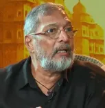
Cabinet Clears Semicon 2.0 at ₹1,27,500 Cr: Kishan Reddy
Synopsis
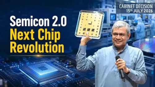
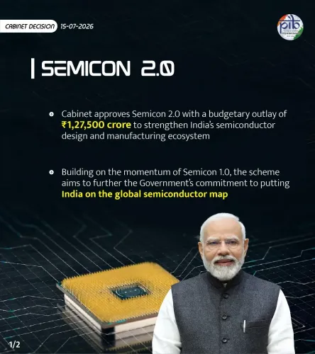
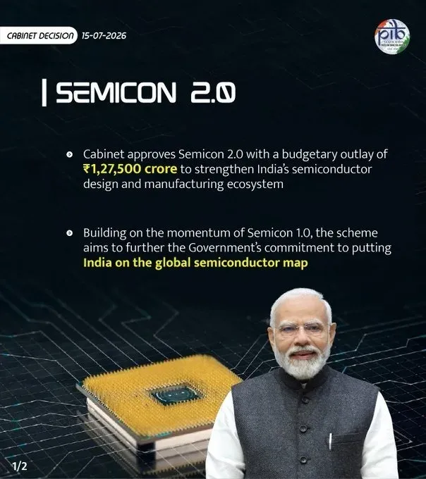
The Union Cabinet has approved Semicon 2.0 with a ₹1,27,500 crore outlay, scaling up India's semiconductor mission to cover chip design, manufacturing, ATMP, OSAT, R&D, and talent development. Union Minister G. Kishan Reddy called it a transformative step toward making India a global semiconductor hub.
Key Takeaways
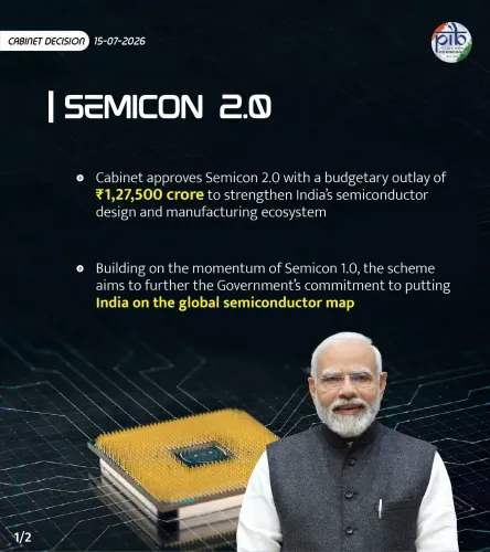
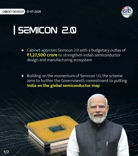
The Union Cabinet , chaired by PM Narendra Modi , approved Semicon 2.0 on 15 July 2026 .
The scheme carries a total budget outlay of ₹1,27,500 crore , up from the original ₹76,000 crore Semicon India programme approved in December 2021 .
Semicon 2.0 covers chip design, semiconductor manufacturing, machines and materials, ATMP, OSAT, R&D, and talent development.
The initiative is positioned under the India Semiconductor Mission and aligned with the goals of Aatmanirbhar Bharat and Viksit Bharat .
The scheme aims to generate high-value employment and position India as a global semiconductor hub.
Next steps include announcement of specific investment proposals and ground-breaking ceremonies for new fabrication and ATMP units.
Union Coal and Mines Minister G. Kishan Reddy on Wednesday, 15 July 2026, welcomed the Union Cabinet's approval of Semicon 2.0, a flagship semiconductor initiative carrying a total budget outlay of ₹1,27,500 crore, describing it as a 'transformative step towards building a robust, self-reliant semiconductor ecosystem in India.'
Context
The cabinet meeting was chaired by Prime Minister Narendra Modi. In his post on X, Kishan Reddy outlined that Semicon 2.0 encompasses chip design, semiconductor manufacturing, machines and materials, advanced ATMP (Assembly, Testing, Marking, and Packaging), OSAT (Outsourced Semiconductor Assembly and Test) facilities, Research and Development, and talent development. The minister said the programme will 'strengthen India's technological capabilities, enhance supply chain resilience, generate high-value employment, and position India as a global semiconductor hub.'
The announcement builds directly on the India Semiconductor Mission, a central government programme established to develop domestic chip design, fabrication, and packaging capabilities since its inception.
Policy Backdrop
India's semiconductor push has a clear policy lineage. In December 2021, the Union Cabinet approved the original Semicon India programme with an outlay of ₹76,000 crore, aimed at attracting semiconductor manufacturing and assembly projects to the country. Semicon 2.0, at ₹1,27,500 crore, represents a significant scaling-up of that ambition — an increase of over ₹51,500 crore from the original programme.
Since 2021, successive policy iterations have combined fiscal support for fabrication units, design-linked incentives, and skill development programmes. The broader objective has been to position India as an alternative semiconductor manufacturing base alongside established hubs in East and Southeast Asia, reducing the country's dependence on chip imports.
Stakeholders and Impact
The scheme is expected to benefit a wide range of stakeholders — from global and domestic semiconductor firms and electronics manufacturers to the engineering and technical workforce seeking high-value employment. The inclusion of ATMP and OSAT facilities is particularly significant, as these segments represent the assembly and testing end of the semiconductor value chain that India has targeted as an early entry point.
Kishan Reddy framed the initiative within the government's twin strategic goals of Aatmanirbhar Bharat (self-reliant India) and Viksit Bharat (developed India), signalling that semiconductor manufacturing is viewed as a cornerstone of India's industrial and technological ambition through the decade.
What's Next
The immediate focus will shift to the announcement of specific investment proposals and ground-breaking ceremonies for new fabrication or ATMP units approved under the expanded outlay. Industry observers will watch for the pace at which domestic and foreign semiconductor firms submit proposals and the timelines set for operationalising new facilities under Semicon 2.0.
With ₹1,27,500 crore now committed, the government's ability to attract anchor investors — particularly global chip giants evaluating India as a manufacturing destination — will be the defining measure of whether the programme delivers on its ambition of making India a credible node in the global semiconductor supply chain.
Point of View
27,500 crore is the most emphatic signal yet that the Modi government views semiconductor self-sufficiency as a non-negotiable pillar of India's industrial strategy, not an aspirational footnote. The near-70 percent jump in outlay from the 2021 programme reflects both the government's assessment that the original scheme built sufficient groundwork and its urgency to compete with the massive state subsidies being deployed by the United States, Europe, Japan, and China. For G. Kishan Reddy — whose portfolio sits outside the technology ministry — amplifying this announcement underscores the BJP's broader political messaging around manufacturing-led growth ahead of state and national electoral cycles. The real test, however, lies ahead: translating a large fiscal commitment into operational fabs and ATMP units within credible timelines, a challenge that has historically separated semiconductor ambition from semiconductor achievement.
NationPress
14 Oct 2026
Frequently Asked Questions
What is Semicon 2.0 and what is its budget?
Semicon 2.0 is the Union Cabinet's expanded semiconductor initiative approved on 15 July 2026, with a total budget outlay of ₹1,27,500 crore. It covers chip design, semiconductor manufacturing, ATMP, OSAT, R&D, and talent development.
How is Semicon 2.0 different from the original Semicon India programme?
The original Semicon India programme was approved in December 2021 with an outlay of ₹76,000 crore. Semicon 2.0 scales this up to ₹1,27,500 crore and broadens the scope to include a more comprehensive end-to-end value chain covering design, fabrication, advanced packaging, and skill development.
What is ATMP and OSAT in the context of India's semiconductor policy?
ATMP stands for Assembly, Testing, Marking, and Packaging, while OSAT stands for Outsourced Semiconductor Assembly and Test. Both refer to the back-end stages of semiconductor manufacturing and are seen as viable early entry points for India into the global chip supply chain.
Who approved Semicon 2.0?
The Union Cabinet, chaired by Prime Minister Narendra Modi, approved Semicon 2.0 on 15 July 2026.
What is the India Semiconductor Mission?
The India Semiconductor Mission is a central government programme established to build domestic semiconductor design, fabrication, and packaging capabilities, under which successive policy initiatives including Semicon India and Semicon 2.0 have been structured.