Cabinet clears Suchi Semicon's ₹868 crore semiconductor project in Gujarat
Synopsis
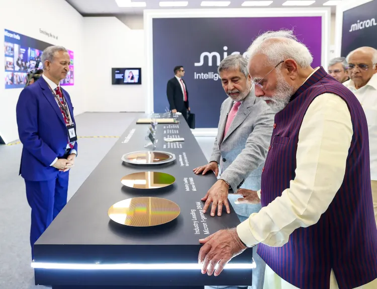
India's semiconductor ambitions gained fresh momentum as the Cabinet cleared two new projects — Suchi Semicon and Crystal Matrix — worth a combined ₹3,936 crore. With the total under the India Semiconductor Mission now at 12, and a Surat OSAT facility capable of churning out over 1,033 million chips annually, the push for self-reliance in a sector critical to defence, mobility, and consumer tech is no longer just policy — it is taking physical shape.
Key Takeaways
The Union Cabinet approved two semiconductor projects — Suchi Semicon (₹868 crore) and Crystal Matrix Limited — with a combined outlay of ₹3,936 crore on 6 May 2025 .
Suchi Semicon is establishing an OSAT facility in Surat, Gujarat with an annual capacity of over 1,033 million chips .
Crystal Matrix will set up a compound semiconductor and Mini/Micro-LED display module manufacturing facility in Dholera, Gujarat , with GaN foundry and six-inch wafer epitaxy services.
The two projects are expected to generate employment for approximately 2,230 skilled professionals .
Total semiconductor projects under the India Semiconductor Mission have now reached 12 .
The Union Cabinet, under Prime Minister Narendra Modi, on Wednesday, 6 May approved two new semiconductor projects — Crystal Matrix Limited and Suchi Semicon — with a combined investment of around ₹3,936 crore, expected to generate employment for approximately 2,230 skilled professionals. Suchi Semicon's project alone carries an outlay of around ₹868 crore and will establish an Outsourced Semiconductor Assembly and Test (OSAT) facility in Surat, Gujarat.
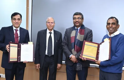
Suchi Semicon's Reaction to Cabinet Approval
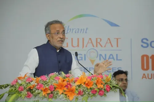
Ashok Mehta, Founder and Chairman of Suchi Semicon, described the Cabinet's nod as a milestone for both the company and the country. "The approval of their project is a proud moment for our organisation and a meaningful contribution to India's larger goal of building indigenous capabilities in a sector of strategic and economic importance," Mehta said in a statement.
Mehta also underscored the strategic imperative behind domestic semiconductor production. "Being able to do this work within India is not just about production — it is about ensuring India is never dependent on others for something so critical," he said, pointing to semiconductors' role in automobiles, industrial machinery, consumer electronics, and defence equipment.
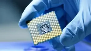
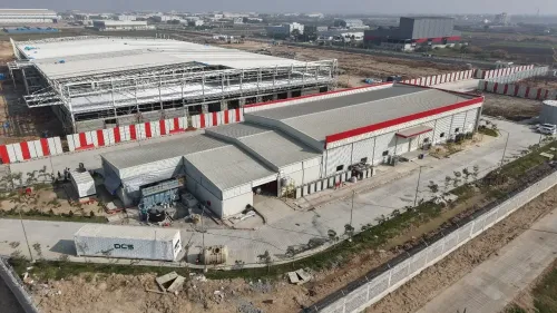
What the Surat OSAT Facility Will Do
Under the India Semiconductor Mission (ISM), Suchi Semicon is setting up its OSAT facility in Surat, Gujarat, with an annual capacity of over 1,033 million chips. The facility will cater to domestic and global demand across power electronics, analog ICs, and industrial systems. Suchi Semicon has stated it remains "fully committed to this national mission and to contributing meaningfully to India's emergence as a trusted, self-reliant semiconductor manufacturing destination."
Crystal Matrix and the Dholera Compound Semiconductor Push
The second approved project, Crystal Matrix Limited, will be located in Dholera, Gujarat, and will focus on compound semiconductor fabrication along with assembly, testing, marking, and packaging (ATMP). Notably, the facility will have a special emphasis on manufacturing Mini/Micro-LED display modules and will offer GaN foundry services, including epitaxy on six-inch wafers. This positions India to serve high-growth segments including smartphones, automotive electronics, televisions, wearables, XR devices, and industrial applications.
India Semiconductor Mission Now Covers 12 Projects
With these two approvals, the total number of semiconductor projects under the India Semiconductor Mission has reached 12, reflecting what officials describe as strong momentum in building a globally competitive and self-reliant semiconductor ecosystem.
Ashok Chandak, President of IESA and SEMI India, said the addition of compound semiconductor-based Mini/Micro-LED manufacturing and OSAT capabilities "will enhance India's position across next-generation technologies, supply chain resilience, innovation, and skilled employment generation." He added that Mini/Micro-LED and epitaxy-based six-inch wafer manufacturing is strategically significant for reducing import dependence in a high-value technology segment.
As India accelerates its semiconductor ambitions, the coming months will be critical in translating Cabinet approvals into operational capacity on the ground.
Point of View
But the harder question is execution velocity. OSAT facilities are the entry-level rung of the semiconductor value chain — essential, but not where the highest strategic leverage lies. India's real test will be whether projects like Crystal Matrix's compound semiconductor and GaN foundry work can graduate from approvals to qualified, export-ready production within competitive timelines. Cabinet clearances have historically outpaced on-ground commissioning in capital-intensive manufacturing. The 2,230-job target is modest relative to the ₹3,936 crore outlay, signalling these are high-skill, low-headcount operations — which is fine for strategic depth, but will not move the mass-employment needle that policymakers often promise alongside such announcements.
NationPress
23 Jun 2026
Frequently Asked Questions
What is the Suchi Semicon semiconductor project approved by the Cabinet?
Suchi Semicon's project is an Outsourced Semiconductor Assembly and Test (OSAT) facility being established in Surat, Gujarat, with an investment of around ₹868 crore under the India Semiconductor Mission. The facility will have a capacity of over 1,033 million chips annually, serving power electronics, analog ICs, and industrial systems.
What is the India Semiconductor Mission and how many projects does it now cover?
The India Semiconductor Mission (ISM) is the Indian government's initiative to build a domestic semiconductor manufacturing ecosystem. With the latest Cabinet approvals of Suchi Semicon and Crystal Matrix Limited, the total number of projects under ISM has reached 12.
What will the Crystal Matrix facility in Dholera produce?
The Crystal Matrix facility in Dholera, Gujarat, will focus on compound semiconductor fabrication and Mini/Micro-LED display module manufacturing. It will also offer GaN foundry services, including epitaxy on six-inch wafers, targeting smartphones, automotive electronics, TVs, wearables, and XR devices.
How many jobs will the two newly approved semiconductor projects create?
The two projects — Suchi Semicon and Crystal Matrix Limited — are together expected to generate employment for approximately 2,230 skilled professionals, according to official statements accompanying the Cabinet approval.
Why is semiconductor self-reliance important for India?
Semiconductors are critical components in defence equipment, automobiles, consumer electronics, and industrial machinery. Domestic production reduces India's dependence on imports and foreign supply chains, which can be disrupted by geopolitical tensions or global shortages, as seen during the COVID-19 pandemic chip crisis.