Semicon 2.0: Cabinet clears ₹1,27,500 crore chip scheme to build India's semiconductor future

Synopsis
India just made its biggest semiconductor bet yet. The Cabinet's ₹1,27,500 crore Semicon 2.0 approval isn't just a funding announcement — it's a six-pillar strategy spanning chip design, fab attraction, advanced packaging, R&D, machines and materials, and talent, built on a first phase that has already pulled in ₹1.64 lakh crore in investment and seen three companies start commercial production.
Key Takeaways
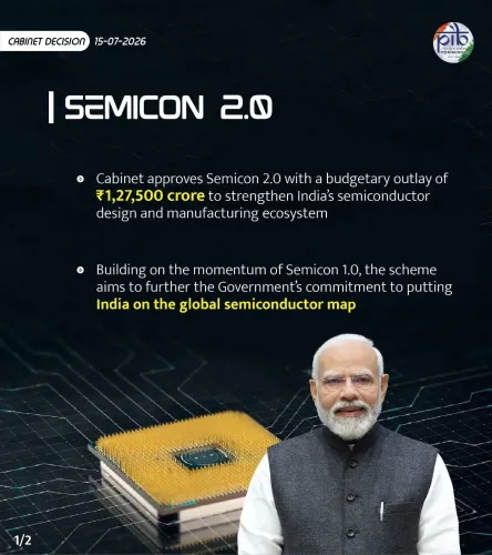
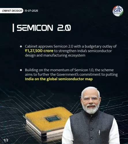
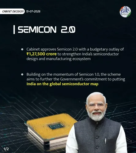
The Union Cabinet approved Semicon 2.0 on 15 July with a ₹1,27,500 crore outlay to build India's semiconductor ecosystem.
Under Semicon 1.0, 12 manufacturing units were approved with cumulative investment exceeding ₹1.64 lakh crore ; Micron , Kaynes , and CG Semi have begun commercial production.
Semicon 2.0 is structured around six pillars : chip design, machines and materials, new fabs, ATMP/OSAT units, R&D, and talent development.
India's first semiconductor fab is scheduled for commissioning in 2028 ; the current node range is 28nm–110nm , with advanced nodes targeted next.
Around 68,000 students across 315 universities have already been trained in chip design using EDA tools under the existing programme.
105 startups and MSMEs have been granted access to industry-standard EDA tools; 24 semiconductor design projects have received financial support.
The Union Cabinet, chaired by Prime Minister Narendra Modi, on Wednesday, 15 July approved the 'Semicon 2.0' scheme, committing a ₹1,27,500 crore outlay to deepen India's domestic semiconductor design and manufacturing ecosystem. The decision builds on the foundation laid by the earlier Semicon 1.0 initiative, which has already drawn over ₹1.64 lakh crore in cumulative investment across 12 approved manufacturing units.
What Semicon 1.0 Has Already Delivered
Under the first phase, the government approved a diverse set of facilities — including one silicon fab, one silicon carbide fab, an integrated gallium nitride micro LED display fab, and nine packaging units. These are expected to serve chip requirements across consumer appliances, industrial electronics, automobiles, power electronics, telecommunications, and aerospace sectors.
Of the 12 approved units, three companies — Micron, Kaynes, and CG Semi — have commenced commercial production, with a fourth expected to begin operations in 2026. Additionally, 24 semiconductor design projects from startups and MSMEs have received financial support, while 105 startups and MSMEs have been granted access to industry-standard Electronic Design Automation (EDA) tools.
The Six Pillars of Semicon 2.0
According to the Cabinet communiqué, Semicon 2.0 is structured around six strategic pillars designed to create a self-sustaining semiconductor ecosystem.
The first pillar focuses on chip design, deepening the ecosystem where 105 startups are already developing chips, with an emphasis on building intellectual property (IP) and system-level designs. The second pillar covers machines and materials — incentivising companies engaged in manufacturing and R&D of semiconductor-grade machines, chemicals, and gases, laying what the Cabinet describes as 'the foundation for sustainable growth' and advancing precision manufacturing in India.
The third pillar targets new fabs. With the first fab scheduled for commissioning in 2028, the government intends to attract additional global manufacturers to establish fabrication units in India. The fourth pillar focuses on ATMP and OSAT units — Assembly, Testing, Marking, and Packaging — where India is increasingly being viewed as an alternative global hub, with the government seeking to attract advanced ATMP technologies.
The fifth pillar is research and development. India's semiconductor journey began at the 28nm–110nm node range; the focus will now shift to more advanced nodes and emerging technologies, pursued in collaboration with leading R&D centres both within and outside India. The sixth pillar is talent development — 315 universities are currently training students in complex chip design using the latest EDA tools, with approximately 68,000 students already trained. The scheme aims to expand this pipeline and deepen the level of training at the undergraduate stage.
Why This Matters for India's Tech Ambitions
Semiconductors are the bedrock of modern technology — from smartphones and electric vehicles to defence systems and data centres. India has historically been a net importer of chips, making it vulnerable to global supply chain disruptions, as starkly exposed during the 2020–2022 chip shortage that paralysed automotive and electronics production worldwide. Semicon 2.0 is the government's most ambitious attempt yet to change that calculus.
Notably, this comes at a moment when the global semiconductor industry is undergoing a significant geographic realignment, with the United States, European Union, Japan, and South Korea all offering large incentives to attract fab investments. India's ₹1,27,500 crore commitment signals that it intends to compete seriously for a place on that map.
What Comes Next
With the Cabinet approval now in place, implementation guidelines and sector-specific incentive structures are expected to be notified in the coming weeks. The semiconductor industry and investor community will watch closely whether the scheme's six pillars translate into binding timelines and verifiable milestones — particularly for the first fab commissioning targeted for 2028.
Point of View
27,500 crore outlay is the right scale for the ambition, but the real test is execution sequencing. India's first fab won't be commissioned until 2028 — three years away — which means the design, materials, and talent pillars must do the heavy lifting in the interim to prevent the ecosystem from stalling at the packaging stage. The global race for semiconductor self-reliance is moving fast: the US CHIPS Act, the EU Chips Act, and Japan's RAPIDUS programme are all ahead of India on fab timelines. What India has is a cost advantage and a growing design talent pool — Semicon 2.0's credibility will hinge on whether those advantages are converted into verifiable IP and advanced-node roadmaps before the 2028 fab window opens.
NationPress
14 Oct 2026
Frequently Asked Questions
What is the Semicon 2.0 scheme approved by the Cabinet?
Semicon 2.0 is a government scheme approved on 15 July by the Union Cabinet, with a ₹1,27,500 crore outlay, aimed at building a comprehensive domestic semiconductor design and manufacturing ecosystem. It succeeds Semicon 1.0 and is structured around six pillars: chip design, machines and materials, new fabs, ATMP/OSAT units, R&D, and talent development.
What has Semicon 1.0 achieved so far?
Under Semicon 1.0, 12 manufacturing units were approved with a cumulative investment of over ₹1.64 lakh crore. Three companies — Micron, Kaynes, and CG Semi — have started commercial production, and a fourth is expected to begin in 2026. Additionally, 24 semiconductor design projects from startups and MSMEs received financial support.
When will India's first semiconductor fab be operational?
India's first silicon fab is scheduled to be commissioned in 2028, according to the Cabinet communiqué. The government is also working to attract additional global manufacturers to set up fabs in India under Semicon 2.0.
Which sectors will benefit from the semiconductor push?
The approved manufacturing units are expected to serve chip requirements across consumer appliances, industrial electronics, automobiles, power electronics, telecommunications, and aerospace. The scheme's broader ambition is to reduce India's dependence on chip imports across all technology-intensive industries.
How is India building semiconductor talent under this scheme?
As of now, approximately 68,000 students across 315 universities have been trained in complex chip design using the latest EDA tools. Semicon 2.0 aims to expand this pipeline and deepen the level of training provided at the college stage.