Cabinet Clears Semicon 2.0 at ₹1,27,500 Cr to Build India Chip Ecosystem
Synopsis
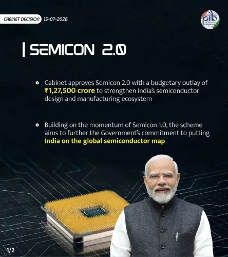
The Union Cabinet chaired by PM Modi has approved Semicon 2.0 with a ₹1,27,500 crore outlay to build India's semiconductor design and manufacturing ecosystem, Science Minister Dr. Jitendra Singh announced on 15 July 2026, marking a major escalation of India's chip self-reliance push.
Key Takeaways
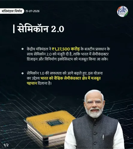
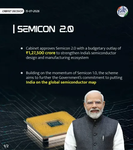
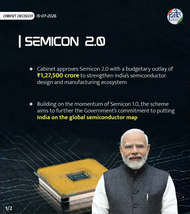
The Union Cabinet approved Semicon 2.0 on 15 July 2026 with a total budget outlay of ₹1,27,500 crore .
The programme targets development of India's semiconductor design and manufacturing ecosystem .
It builds on the original Semicon India programme approved in December 2021 with an outlay of ₹76,000 crore .
The announcement was made by Union Minister Dr.
Jitendra Singh via his official X account.
Key stakeholders include semiconductor firms , electronics manufacturers , and the STEM workforce .
The programme aligns with Atmanirbhar Bharat and Make in India goals of reducing chip import dependence.
Union Science and Technology Minister Dr. Jitendra Singh announced on Wednesday, 15 July 2026 that the Union Cabinet, chaired by Prime Minister Narendra Modi, has approved Semicon 2.0 — a landmark programme to develop India's semiconductor design and manufacturing ecosystem with a total budget outlay of ₹1,27,500 crore.
Context
Dr. Jitendra Singh shared the Cabinet decision on X (formerly Twitter), stating that the programme 'aims to further Government's commitment towards putting our country on the semiconductor map of the world.' The announcement positions Semicon 2.0 as a significant escalation of India's existing semiconductor push, both in ambition and in financial firepower.
The outlay of ₹1,27,500 crore marks a substantial step up from the ₹76,000 crore committed under the original Semicon India programme approved by the Union Cabinet in December 2021. That earlier scheme laid the groundwork for semiconductor fabrication units and an ecosystem development fund, establishing the institutional scaffolding that Semicon 2.0 now builds upon.
Policy Backdrop
India's semiconductor drive is rooted in the broader Atmanirbhar Bharat and Make in India frameworks championed by Prime Minister Modi since 2014. The India Semiconductor Mission, launched in 2021 under the Ministry of Electronics and IT, was designed to attract investment into chip design, fabrication, and packaging — the three pillars of a self-sufficient semiconductor value chain.
The global context has been equally compelling. Pandemic-era supply-chain disruptions and mounting geopolitical tensions around Taiwan and China exposed the vulnerabilities of countries heavily dependent on imported chips. Successive Union Budgets have incrementally raised committed funding while broadening the scope to cover upstream design as well as downstream assembly, testing, and packaging — known in the industry as OSAT (Outsourced Semiconductor Assembly and Test) capacity.
Semicon 2.0 appears to consolidate these threads into a single, scaled-up programme, signalling that the government views semiconductor self-reliance not as a pilot initiative but as a core industrial policy priority for the decade ahead.
Stakeholders and Impact
The programme's beneficiaries span the full length of the electronics value chain. Semiconductor design firms — both domestic startups and global fabless companies — stand to gain from enhanced incentives and a deeper local talent pool. Electronics manufacturers that currently import chips for consumer goods, defence systems, and automotive applications could see supply-chain costs and risks reduced over time.
The STEM workforce is another critical stakeholder. A programme of this scale is expected to generate demand for chip designers, process engineers, and packaging specialists — disciplines that Indian universities and technical institutes are increasingly being called upon to supply. The announcement is likely to spur fresh curriculum and research investment at institutions aligned with the mission.
For global chipmakers and equipment suppliers evaluating India as a manufacturing destination, the enhanced outlay sends a clear signal of policy continuity and government commitment — factors that weigh heavily in multi-billion-dollar investment decisions with decade-long payback horizons.
What's Next
Attention will now turn to the rollout details: which fabrication and OSAT projects will be greenlit under the revised outlay, what the revised incentive structure looks like for applicants, and whether fresh investment proposals will be unveiled at the next Semicon India summit. Implementation timelines and the role of state governments in land and infrastructure support will also be closely watched.
With ₹1,27,500 crore now committed, India's semiconductor ambitions have moved decisively from aspiration to policy architecture — and the world's chip industry will be watching to see how quickly that architecture translates into silicon on the ground.
Point of View
27,500 crore — nearly 68 per cent higher than the original Semicon India outlay — signals that the Modi government is treating semiconductor self-reliance as a generational industrial bet, not an incremental subsidy scheme. The timing is strategically astute: as the United States, European Union, and Japan pour public money into domestic chip capacity, India is positioning itself to capture supply-chain diversification flows from companies unwilling to concentrate risk in Taiwan or China. The scale of the outlay also raises the political stakes — delivery on fabrication milestones will be scrutinised as a test of whether India's industrial policy ambitions can match its financial commitments. Dr. Jitendra Singh's role in anchoring the announcement underscores the Science and Technology Ministry's growing centrality to India's economic strategy.
NationPress
14 Oct 2026
Frequently Asked Questions
What is Semicon 2.0 India?
Semicon 2.0 is a Union Cabinet-approved programme aimed at developing India's semiconductor design and manufacturing ecosystem, with a total budget outlay of ₹1,27,500 crore. It was approved on 15 July 2026 and builds on the original Semicon India programme launched in 2021.
What is the budget of Semicon 2.0?
The Union Cabinet has approved a total budget outlay of ₹1,27,500 crore for Semicon 2.0. This is significantly higher than the ₹76,000 crore committed under the original Semicon India programme in December 2021.
What is the India Semiconductor Mission?
The India Semiconductor Mission is a central government initiative launched in 2021 to build semiconductor design, fabrication, and packaging capacity in India. Semicon 2.0 is the next phase of this broader national semiconductor push.
Who announced Semicon 2.0?
Union Minister of State (Independent Charge) for Science and Technology Dr. Jitendra Singh announced the Cabinet approval of Semicon 2.0 on 15 July 2026 via his official post on X.
How does Semicon 2.0 help India reduce chip imports?
By funding semiconductor design, fabrication, and packaging capacity within India, Semicon 2.0 aims to reduce India's dependence on imported chips. The programme offers production-linked incentives and state support for fabs and OSAT units, making India more competitive in global semiconductor supply chains.