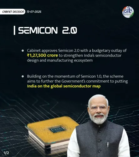
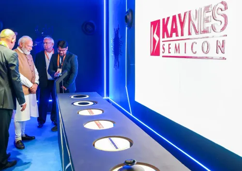
Semicon 2.0: India targets indigenous chip IP and global scale with ₹1,27,500 crore push
Synopsis
India's Semicon 2.0 — backed by ₹1,27,500 crore — marks a decisive shift from building design infrastructure to producing globally competitive, Indian-owned chip products. With 12 manufacturing units already approved and over ₹1.64 lakh crore committed, the question now is whether India can convert design talent into commercially dominant semiconductor brands.
Key Takeaways
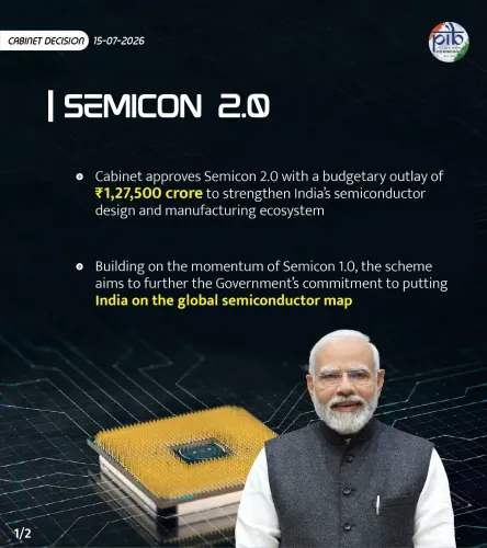
The government approved Semicon 2.0 with a total outlay of ₹1,27,500 crore to develop a domestic semiconductor design and manufacturing ecosystem.
ISM 1.0 expanded EDA tool access to over 340 institutions and supported semiconductor startups across India.
12 manufacturing units have been approved to date, with cumulative investment exceeding ₹1.64 lakh crore .
Krishnan said the focus is on scaling Indian firms, strengthening indigenous IP, and attracting private investment.
Target sectors include mobile phones, consumer electronics, automotive, EV, IT hardware, and data centres.
The scheme aims to position India as a leading global semiconductor product nation , with chips designed, owned, and commercialised from India.
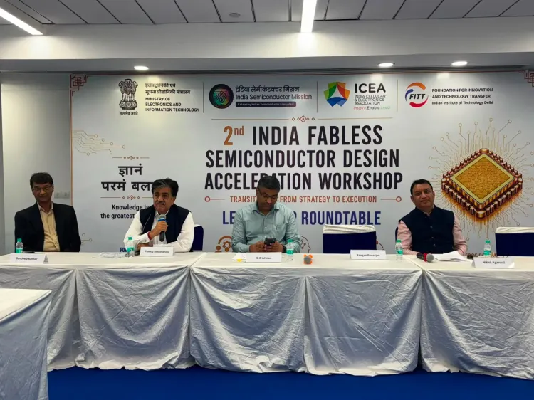
India's Semicon 2.0 scheme, approved by the government this month with a total outlay of ₹1,27,500 crore, is designed to help Indian semiconductor firms scale operations, strengthen indigenous intellectual property, and convert world-class chip design into globally competitive products, IT Secretary S. Krishnan said on Friday, 31 July. Speaking at the second India Fabless Semiconductor Design Acceleration Workshop at IIT Delhi, Krishnan outlined the government's ambitions for the next phase of India's semiconductor journey.
From Foundation to Scale
The first phase — ISM 1.0 — laid the groundwork by expanding access to Electronic Design Automation (EDA) tools across more than 340 institutions, nurturing startups, and seeding a domestic innovation ecosystem. Semicon 2.0 now builds on that base with a sharper commercial mandate.
'Our focus is to help Indian companies scale, strengthen indigenous intellectual property, attract greater private investment, and, most importantly, transform world-class chip design into globally competitive products,' Krishnan said at the event.
What Semicon 2.0 Covers
To date, 12 manufacturing units have been approved under India's semiconductor programme, with a cumulative investment of over ₹1.64 lakh crore. The expanded Semicon 2.0 framework is intended to bring in startups, established companies, overseas collaborators, and investors into a more inclusive ecosystem.
Amitesh Kumar Sinha, CEO of the India Semiconductor Mission (ISM), said the new phase would strengthen long-term financing, improve market access, and support the transition from chip design to commercial products. 'We are laying the foundation for globally competitive Indian semiconductor companies,' Sinha noted.
Target Sectors and Industry Priorities
The workshop deliberated on building indigenous semiconductor products for high-growth sectors including mobile phones and wearables, consumer electronics and televisions, air conditioners and home appliances, IT hardware and data centres, and automotive and electric vehicles.
Pankaj Mohindroo, Chairman of the India Cellular and Electronics Association (ICEA) — which organised the event in collaboration with FITT, IIT Delhi — said the next phase must focus on creating Indian-owned semiconductor products, IP, and globally competitive technology companies. 'As India's electronics manufacturing ecosystem expands rapidly, semiconductor development must be driven by the needs of sectors such as mobile phones, consumer electronics, automotive, IT hardware, telecom, industrial electronics and power electronics,' he said.
The Broader Ambition
Krishnan underscored the government's commitment to building enabling infrastructure, expanding access to cutting-edge design tools, and creating conditions for industry-academia collaboration. 'Together, we must ensure that India's semiconductor capabilities translate into products designed, owned, and commercialised from India, positioning the country as a leading global semiconductor product nation,' he said.
This comes amid a global scramble for semiconductor self-sufficiency, with the US, European Union, Japan, and China each deploying multi-billion-dollar chip incentive programmes. India's push, if executed at scale, could position it as a credible alternative hub — particularly in fabless chip design, where capital requirements are lower than in fabrication.
Point of View
Yet, is a single Indian-owned chip brand with global market share. The ₹1,27,500 crore outlay signals intent, but semiconductor ecosystems are won on execution timelines measured in decades, not policy cycles. India's fabless ambition is credible on paper; the test is whether the transition from design capability to commercial product — the graveyard of many chip programmes globally — can be navigated with the private-sector pull that government schemes alone cannot manufacture.
NationPress
15 Sept 2026
Frequently Asked Questions
What is India's Semicon 2.0 scheme?
Semicon 2.0 is a government-approved scheme with a total outlay of ₹1,27,500 crore aimed at developing India's domestic semiconductor design and manufacturing ecosystem. It builds on ISM 1.0 by focusing on scaling Indian firms, strengthening indigenous intellectual property, and converting chip design capabilities into globally competitive products.
How does Semicon 2.0 differ from ISM 1.0?
ISM 1.0 focused on building foundational infrastructure — expanding EDA tool access to over 340 institutions and supporting startups. Semicon 2.0 shifts the emphasis to commercial scale, indigenous IP ownership, long-term financing, and market access, with the goal of producing globally competitive Indian semiconductor products.
How many semiconductor manufacturing units has India approved so far?
As of 31 July, 12 semiconductor manufacturing units have been approved in India, with a cumulative investment of over ₹1.64 lakh crore across these projects.
Which sectors will benefit from Semicon 2.0?
The scheme targets high-growth sectors including mobile phones and wearables, consumer electronics, air conditioners and home appliances, IT hardware and data centres, and automotive and electric vehicles, among others.
Who are the key stakeholders involved in Semicon 2.0?
Key stakeholders include the India Semiconductor Mission (ISM), led by CEO Amitesh Kumar Sinha, the India Cellular and Electronics Association (ICEA), chaired by Pankaj Mohindroo, and IIT Delhi's FITT. The scheme is overseen by the Ministry of Electronics and IT, with IT Secretary S. Krishnan as a leading voice.