India Semiconductor Mission 2.0 spawns 200 chip design firms, 70,000 engineers trained
Synopsis
India Semiconductor Mission 2.0 has quietly built an ecosystem: 200 chip design companies, 105 startups with EDA tool access, 20 VC-backed ventures, and 70,000 trained engineers — all in four years. With five ISM 1.0 plants now in commercial production and major economies circling at SEMICON India 2026, India's semiconductor ambitions are shifting from policy announcement to measurable output.
Key Takeaways
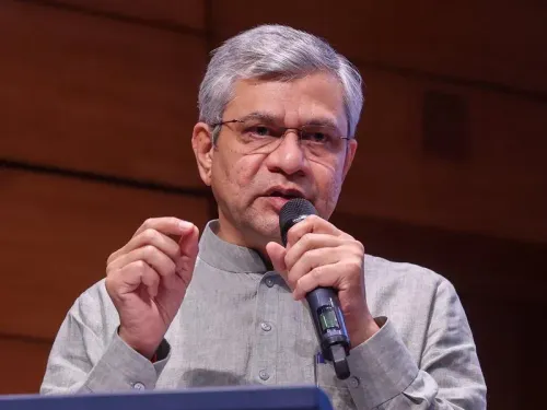
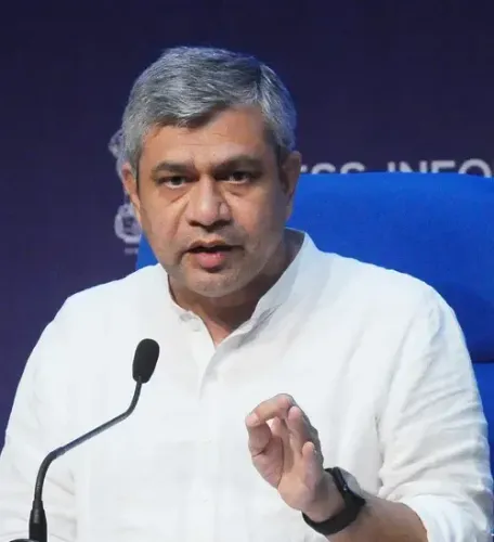
200 chip design companies have emerged under India Semiconductor Mission 2.0 (ISM 2.0) , according to Minister Ashwini Vaishnaw .
More than 105 chip design startups received access to Electronic Design Automation (EDA) tools; 20 startups have secured venture capital funding.
Approximately 70,000 chip-design engineers trained over four years , against a target of 85,000 .
Five of 12 plants approved under ISM 1.0 have begun commercial production.
SEMICON India 2026 country roundtables drew 142 participants (India–Singapore), 139 (India–Europe), and 115 (India–South Korea).
Foreign Secretary Vikram Misri called for trusted global partnerships as the backbone of resilient semiconductor value chains.
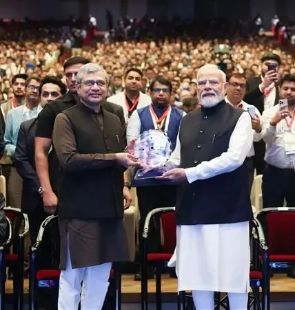
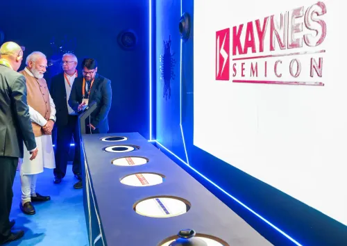
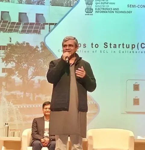
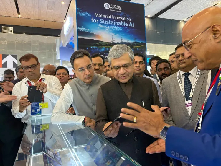
India Semiconductor Mission 2.0 (ISM 2.0) has given rise to at least 200 chip design companies, marking what Union Minister for Electronics and IT Ashwini Vaishnaw described as a 'game changer' for building home-grown semiconductor intellectual property (IP). The figures, shared during SEMICON India 2026 in New Delhi, underscore the country's accelerating push to position itself as a credible node in the global semiconductor value chain.
Startups, Funding and Engineering Talent
More than 105 chip design startups have gained access to state-of-the-art Electronic Design Automation (EDA) tools under the mission, with 20 startups going on to secure venture capital funding. The minister also noted that approximately 70,000 chip-design engineers have been trained over the past four years, against a target of 85,000 — placing the programme at roughly 82% of its training goal.
Manufacturing Progress Under ISM 1.0
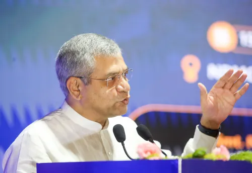
Vaishnaw highlighted that five of the 12 plants approved under ISM 1.0 have commenced commercial production, signalling a gradual transition from planning to output. He stressed that global competitiveness in semiconductors demands both quality and competitive cost — a dual benchmark India is working to meet. The minister also underlined India's status as a trusted partner nation with a strong record in intellectual property protection, positioning the country as a reliable destination for sensitive technology investments.
Global Partnerships at SEMICON India 2026
Foreign Secretary Vikram Misri reinforced the geopolitical dimension of semiconductor supply chains, arguing that resilience requires trusted global partnerships built on reliability, credibility, incentives, and value creation. He called for a balanced approach that combines domestic strengths with global capabilities rather than pursuing self-reliance in isolation.
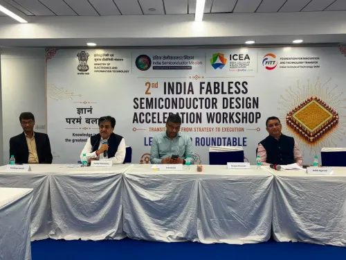
The event hosted several high-attendance country roundtables. The India–Singapore Country Roundtable drew 142 participants and explored how Singapore's manufacturing, advanced packaging, and supply-chain expertise could complement India's engineering talent and expanding ecosystem. The India–Europe Country Roundtable, attended by 139 participants, focused on investment, supply-chain localisation, equipment and materials, manufacturing, advanced packaging, design, R&D, and talent development. The India–South Korea Country Roundtable brought together 115 participants to identify opportunities across the semiconductor value chain, pairing South Korea's established capabilities with India's engineering base and growing market scale.
Why This Milestone Matters
This comes amid a global scramble to diversify semiconductor supply chains away from dependence on a handful of East Asian manufacturers. India's twin advantages — a large pool of engineering graduates and a cost structure competitive with other emerging semiconductor hubs — have drawn renewed attention from chipmakers and equipment suppliers alike. Notably, the emergence of 200 chip design companies in a relatively short window suggests that ISM 2.0's EDA tool access and funding pathways are beginning to convert engineering talent into commercial IP creation. The critical next test is whether domestic design wins translate into actual tape-outs and licensing revenues, closing the gap between skill formation and industrial-scale output.
With SEMICON India 2026 generating extensive business-to-business engagement and significant participation from major semiconductor economies, the stage appears set for a sharper phase of investment announcements in the months ahead.
Point of View
Not factories. The real metric India needs to track is how many of these firms have secured licensing deals or production contracts, not just EDA access. The 70,000 engineers trained figure is impressive until you note it is still 15,000 short of the stated target with four years elapsed. And with only five of twelve ISM 1.0 plants in commercial production, the gap between approval and output remains wide. India's semiconductor story is real, but the distance between ecosystem formation and supply-chain relevance is still measured in years and billions of dollars of sustained capital.
NationPress
19 Sept 2026
Frequently Asked Questions
What is India Semiconductor Mission 2.0 (ISM 2.0)?
India Semiconductor Mission 2.0 is the government's expanded programme to build a domestic semiconductor ecosystem, covering chip design, manufacturing, and talent development. Under ISM 2.0, at least 200 chip design companies have emerged and more than 105 startups have received access to Electronic Design Automation tools.
How many engineers has India trained under ISM 2.0?
Approximately 70,000 chip-design engineers have been trained over four years under the mission, against a stated target of 85,000. The government has not specified a revised deadline for closing the remaining gap.
How many semiconductor plants are operational under ISM 1.0?
Five of the twelve plants approved under ISM 1.0 have commenced commercial production, according to Minister Ashwini Vaishnaw. The remaining seven are at various stages of development.
What was discussed at SEMICON India 2026?
SEMICON India 2026 hosted country roundtables with Singapore (142 participants), Europe (139 participants), and South Korea (115 participants), focusing on manufacturing, advanced packaging, supply-chain localisation, chip design, R&D, and investment opportunities. Foreign Secretary Vikram Misri emphasised trusted global partnerships as essential to resilient semiconductor supply chains.
Why is India's semiconductor push strategically significant?
Global supply chains are under pressure to diversify away from dependence on a narrow set of East Asian chipmakers. India's combination of engineering talent, competitive costs, and growing incentive frameworks has drawn interest from major semiconductor economies, as demonstrated by the strong international turnout at SEMICON India 2026.