Can India Emerge as a Global Semiconductor Power?
Synopsis
India is on a mission to become a leading global semiconductor power, as emphasized by Union Minister Ashwini Vaishnaw. The nation is striving for self-reliance in strategic sectors by leveraging indigenous chip technology, with innovative programs engaging academic institutions. This initiative is pivotal for India's future in the semiconductor industry.
Key Takeaways
Self-Reliance: India aims to achieve independence in semiconductor technology.
Chips to Start-up: Engaging students in practical chip design.
ChipIN Centre: A centralized facility for advanced semiconductor design.
Significant Fabrication: 56 chips fabricated from student designs.
Global Leadership: India is emerging as a leader in the semiconductor landscape.
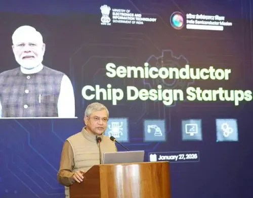
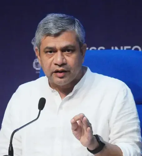
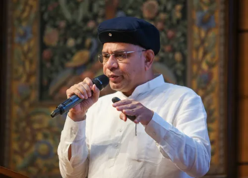
New Delhi, Nov 30 (NationPress) India needs to develop capabilities of significant scale and strength to position itself as a prominent global semiconductor player within the next few years, stated Union Minister Ashwini Vaishnaw.
He emphasized the goal is to achieve self-reliance in strategic sectors and reduce dependency on external sources for essential needs, advocating for the use of indigenous chips.
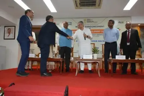
The minister presented 28 chips, which were manufactured at the Semiconductor Laboratory (SCL) in Mohali, including 600 bare dies and 600 packaged chips, produced by students from 17 academic institutions through the Chips to Start-up (C2S) Programme.
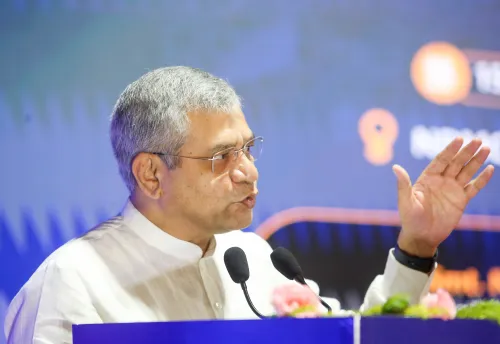
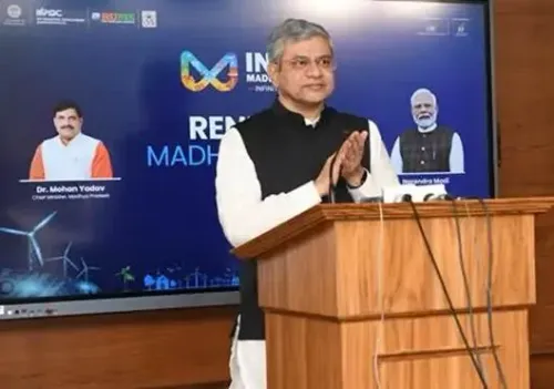
According to him, India is swiftly becoming a noteworthy leader in the global semiconductor arena.
“Currently, various institutions nationwide have access to some of the leading design technologies, fostering a large-scale semiconductor development ecosystem unique to India,” noted Vaishnaw.
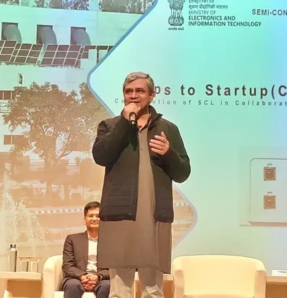
The ChipIN Centre, which is among the largest facilities established at C-DAC Bangalore, provides an extensive array of semiconductor design workflows and solutions, aiming to connect national chip design infrastructure directly with the semiconductor design community across India.
This centralized facility is equipped with the most advanced tools for the entire chip design cycle.
It also provides compute and hardware infrastructure, IP cores, and mentorship, delivering comprehensive services for design fabrication at the SCL foundry and packaging for academic institutions participating in the C2S Programme of the Ministry of Electronics and Information Technology.
The ChipIN Centre collects chip designs created by students from C2S Programme institutions.
Every three months, these designs are compiled and sent to SCL Mohali for fabrication using 180 nm technology.
Once approved, the designs are merged onto a single mask (MPW reticle) by the ChipIN Centre, which optimizes both time and cost by manufacturing multiple designs in one run.
SCL Mohali then fabricates, packages, and delivers the chips back to the students.
In the last year, the ChipIN Centre conducted 5 MPW shuttle runs for fabrication of designs at SCL under the C2S programme.
A total of 122 designs were submitted by 46 institutions across India. Among these, SCL has successfully fabricated 56 student-designed chips and delivered them to their respective institutions, according to the ministry.
Point of View
It is essential to recognize India's strategic push towards semiconductor self-sufficiency. This initiative reflects a broader vision for technological independence, aiming to reduce reliance on foreign technologies. Such advancements are crucial for national security and economic growth.
NationPress
30 Jun 2026
Frequently Asked Questions
Why is India focusing on semiconductor development?
India is aiming to become self-reliant in strategic sectors, reducing dependency on foreign technologies and ensuring national security.
What is the Chips to Start-up (C2S) Programme?
The C2S Programme engages academic institutions in semiconductor design, allowing students to contribute to India's chip development efforts.
What role does the ChipIN Centre play?
The ChipIN Centre provides a comprehensive semiconductor design infrastructure, facilitating access to advanced tools and mentorship for students and institutions.
How many designs have been fabricated under the C2S Programme?
A total of 56 student-designed chips have been successfully fabricated and delivered to various institutions across India.
What technology is being used for chip fabrication?
The designs are fabricated using 180 nm technology at the Semiconductor Laboratory in Mohali.