South Korea chip cluster: Lee Jae Myung pushes ₩800 trillion semiconductor drive
Synopsis
South Korea is betting its economic future on a ₩800 trillion chip-and-AI blitz — and President Lee Jae Myung isn't waiting for paperwork to catch up. By ordering all regulatory reviews to run simultaneously and infrastructure planning to begin immediately, Lee is signalling that Seoul intends to outpace the US, Taiwan, and Japan in the global semiconductor race, not just match them.
Key Takeaways
President Lee Jae Myung on 7 July 2025 directed officials and chipmakers to fast-track South Korea's chip cluster and AI investment programme.
Samsung Electronics and SK hynix have jointly pledged ₩800 trillion (US$522 billion) for a semiconductor production cluster in the Honam region .
The 'three mega projects' initiative spans semiconductors , physical AI , and AI data centres .
Lee ordered all mandatory administrative procedures — including environmental impact reviews — to run simultaneously rather than sequentially.
Planning for electricity and water supply for the chip cluster is to begin immediately, without waiting for other clearances.
Site selection for the investment projects was flagged as an urgent deliverable at the meeting.
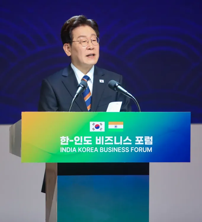
South Korean President Lee Jae Myung on Monday, 7 July 2025, directed senior government officials and top executives of Samsung Electronics and SK hynix to fast-track the country's landmark chip cluster and AI investment programme, calling for administrative procedures — including mandatory environmental impact reviews — to be run concurrently rather than sequentially. The directive came at a high-level meeting convened to chart follow-up action on the recently announced 'three mega projects' initiative.
What the Three Mega Projects Cover
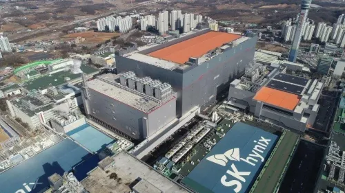
Unveiled last week, the initiative centres on large-scale state-backed investments across three domains: semiconductor manufacturing, physical artificial intelligence (AI), and AI data centres. The centrepiece is a planned semiconductor production cluster in the southwestern Honam region, for which Samsung Electronics and SK hynix have together pledged a combined 800 trillion won (approximately US$522 billion) — one of the largest industrial investment commitments in South Korean history.
Lee's Directive: Speed Over Sequence
'The world is witnessing very intense competition, while an entirely new future is being shaped around AI,' President Lee said in his opening remarks at the meeting. 'At a time when all-out competition that will determine the nation's fate is under way, who moves first and who moves faster will be the deciding factor,' he added.
Lee specifically called on the government to pre-emptively identify and remove obstacles before they arise, so that chipmakers can concentrate entirely on investment and operations. 'Investments should never be delayed because of delays in administrative procedures,' he said. He also directed that efforts to secure electricity and water supplies for the envisioned cluster begin immediately, without waiting for other preliminary clearances to conclude.
Why Administrative Speed Matters Here
South Korea's regulatory framework typically requires environmental impact assessments to be completed in a fixed sequence before construction permits are granted. For a project of this scale — spanning a new industrial zone in the Honam area — that process could add months or years to the timeline. By mandating parallel processing of all mandatory reviews, Lee is signalling that Seoul will not allow procedural bottlenecks to cede ground to rivals. This comes amid intensifying global competition from the United States, Taiwan, and Japan, each of which has committed hundreds of billions of dollars to domestic semiconductor capacity in recent years.
Samsung, SK Hynix and the Stakes for South Korea
The combined ₩800 trillion pledge from Samsung and SK hynix underscores the strategic weight Seoul is placing on advanced chips and AI infrastructure. South Korea's semiconductor sector already accounts for a significant share of its export earnings, and the new cluster is designed to deepen that advantage — particularly in memory chips and next-generation AI accelerators. Officials at the meeting were also asked to swiftly finalise the specific sites that will host the investment projects, with site selection now treated as an urgent deliverable.
What Comes Next
The immediate priorities, per the president's instructions, include streamlining environmental reviews, locking down site locations, and initiating parallel infrastructure planning for power and water. Industry observers will watch whether the regulatory fast-tracking translates into ground-breaking timelines that match the ambition of the ₩800 trillion commitment. South Korea's ability to execute at speed — not just announce at scale — will be the defining test of this initiative.
Point of View
But the harder question is whether Seoul's regulatory machinery can actually be compressed without cutting corners on environmental and safety assessments that exist for good reason. Lee's parallel-processing directive is politically bold — but fast-tracking environmental reviews for a massive industrial cluster in the Honam region carries real ecological risk that deserves scrutiny, not just applause. More broadly, South Korea is the third major economy this year to announce a nine-figure semiconductor commitment; the race is real, but so is the risk of overcapacity if the US, Japan, Taiwan, and Korea all build to full ambition simultaneously. The execution discipline of Samsung and SK hynix is not in doubt — the open variable is whether the state can deliver the infrastructure and regulatory speed that Lee has promised.
NationPress
5 Oct 2026
Frequently Asked Questions
What is South Korea's semiconductor chip cluster project?
It is a large-scale semiconductor production facility planned for the southwestern Honam region of South Korea, backed by a combined investment pledge of ₩800 trillion (US$522 billion) from Samsung Electronics and SK hynix. It forms the centrepiece of the government's 'three mega projects' initiative alongside physical AI and AI data centre investments.
Why is President Lee Jae Myung pushing to fast-track the chip cluster?
Lee has cited intensifying global competition in AI and semiconductors, arguing that speed of execution will be the decisive factor in determining which nation leads these industries. He has directed that administrative reviews run simultaneously rather than sequentially to prevent procedural delays from stalling investment.
How much are Samsung and SK hynix investing in the chip cluster?
Samsung Electronics and SK hynix have together pledged a combined ₩800 trillion, equivalent to approximately US$522 billion, making it one of the largest industrial investment commitments in South Korean history.
What are the 'three mega projects' announced by the South Korean government?
The three mega projects cover large-scale investments in semiconductor manufacturing, physical artificial intelligence, and AI data centres. The initiative was unveiled last week and is designed to position South Korea as a global leader in advanced industries.
What infrastructure steps have been ordered for the chip cluster?
President Lee has directed that planning to secure electricity and water supplies for the chip cluster begin immediately, without waiting for other preliminary procedures to be completed. Site selection for all investment projects has also been designated an urgent priority.