CM Rekha Gupta Backs ₹1,27,500 Cr Semicon 2.0 Cabinet Nod
Synopsis
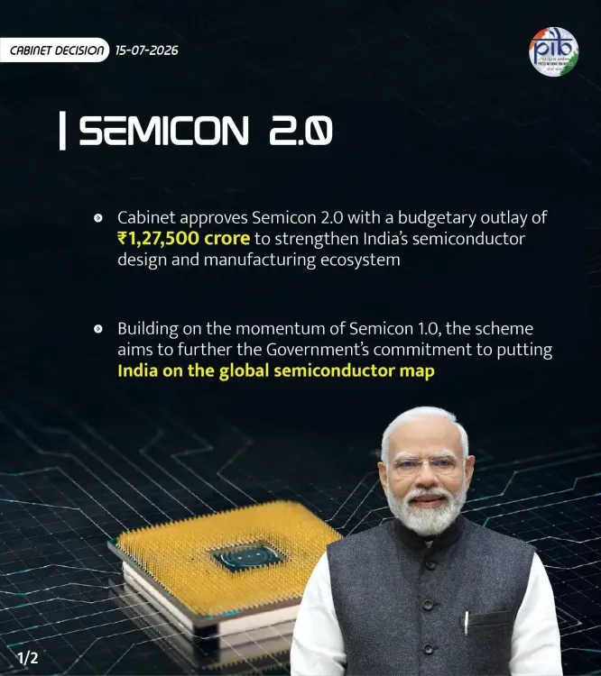
Delhi Chief Minister Rekha Gupta has backed the Union Cabinet's approval of the ₹1,27,500 crore Semicon 2.0 programme, calling it a historic decision and pledging to make Delhi a national leader in chip design, research, and advanced technology.
Key Takeaways
The Union Cabinet approved the Semicon 2.0 programme with a total outlay of ₹1,27,500 crore under PM Narendra Modi .
Delhi CM Rekha Gupta described the decision as historic and said it would strengthen India's technological self-reliance.
Delhi aims to become a leading national centre for chip design, R&D, innovation, and advanced technology under this programme.
Semicon 2.0 expands on the India Semiconductor Mission launched in December 2021 with an initial outlay of ₹76,000 crore .
The programme is part of the Atmanirbhar Bharat framework to reduce India's semiconductor import dependence.
Key next steps include project approvals, fund disbursement to Delhi design centres, and potential MoUs with global chip firms.
Delhi Chief Minister Rekha Gupta on Wednesday, 15 July 2026 welcomed the Union Cabinet's approval of the Semicon 2.0 programme, a landmark semiconductor initiative with an outlay of ₹1,27,500 crore, describing it as a historic decision that will strengthen India's technological self-reliance and power the economy of the future.
Context
Posting on X, CM Rekha Gupta said the Cabinet decision, taken under the leadership of Prime Minister Narendra Modi, was an 'ऐतिहासिक निर्णय' ('historic decision') that would give new energy to India's technological self-reliance. She added that the move would give fresh momentum to Delhi's semiconductor vision, reinforcing the capital's resolve to become a leading centre for chip design, research, innovation, and advanced technology.
The Chief Minister's remarks come as the Union Cabinet formally cleared the expanded semiconductor programme, scaling up fiscal support well beyond the initial outlay committed under earlier national semiconductor initiatives.
Policy Backdrop
India's semiconductor push has been building since December 2021, when the Union Cabinet approved the India Semiconductor Mission with an initial outlay of ₹76,000 crore to attract investment in fabrication, assembly, testing, and design. Semicon 2.0 represents a significant expansion of that framework, raising the total committed outlay to ₹1,27,500 crore.
The programme sits within the broader Atmanirbhar Bharat framework, which has sought to reduce India's heavy dependence on semiconductor imports and integrate domestic industry into global chip supply chains. Successive Cabinet decisions have progressively enlarged fiscal support across the semiconductor value chain.
Stakeholders and Impact
The semiconductor industry, Delhi's technology ecosystem, and research institutions are among the primary stakeholders expected to benefit from the programme. CM Gupta specifically highlighted chip design, research, innovation, and advanced technology as the domains where the capital aims to emerge as a front-runner.
For Delhi, which lacks the large land parcels required for fabrication plants, the emphasis on design and R&D clusters aligns with the city's existing strengths in engineering talent and academic institutions. A national programme of this scale could accelerate the formation of design centres and start-up clusters in the capital.
What's Next
Attention will now turn to the rollout of specific project approvals, disbursement of funds to Delhi-based design centres, and potential new agreements with global chip firms in the coming fiscal year. CM Gupta's statement signals that the Delhi government intends to actively position the capital to capture design and innovation mandates under the expanded national programme.
If the programme's implementation proceeds on schedule, Semicon 2.0 could mark a structural shift in India's position within the global semiconductor value chain, with Delhi aiming to anchor the design and R&D end of that chain.
Point of View
She signals that the BJP-led state government is aligned with — and intends to benefit from — the Modi administration's flagship technology agenda. The statement shifts Delhi's role in the semiconductor narrative from passive recipient to active claimant of design and R&D mandates. At a time when states are competing for semiconductor investment, staking a design-hub identity early could shape how central allocations are directed. This is as much about inter-state competition for high-value tech jobs as it is about national self-reliance.
NationPress
15 Jul 2026
Frequently Asked Questions
What is the Semicon 2.0 programme approved by the Cabinet?
Semicon 2.0 is a Union Cabinet-approved semiconductor programme with a total outlay of ₹1,27,500 crore, aimed at expanding India's chip design, research, and manufacturing capabilities under the Atmanirbhar Bharat framework.
What did Delhi CM Rekha Gupta say about Semicon 2.0?
CM Rekha Gupta called the Cabinet approval a historic decision that would give new momentum to Delhi's semiconductor vision and strengthen the capital's resolve to become a leading centre for chip design, innovation, and advanced technology.
How does Semicon 2.0 differ from the India Semiconductor Mission?
The India Semiconductor Mission was launched in December 2021 with an initial outlay of ₹76,000 crore. Semicon 2.0 represents a significant expansion, raising the committed outlay to ₹1,27,500 crore with a broader focus on design and R&D alongside manufacturing.
What is Delhi's role in India's semiconductor ambitions?
Delhi aims to become a national hub for chip design, research, and advanced technology rather than fabrication, leveraging its engineering talent and academic institutions to anchor the design end of the semiconductor value chain.
What happens next after the Semicon 2.0 Cabinet approval?
The next steps include rollout of specific project approvals, disbursement of funds to design centres including those in Delhi, and potential agreements with global semiconductor firms in the coming fiscal year.