CM Samrat Choudhary backs Semicon 2.0 with ₹1.27 lakh cr push
Synopsis
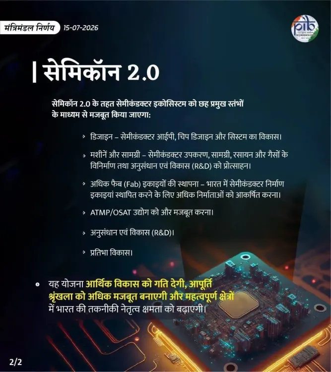
Bihar Chief Minister Samrat Choudhary has endorsed the Union Cabinet's Semicon 2.0 Mission, backed by a ₹1,27,500 crore outlay, saying it will strengthen India's semiconductor design, manufacturing, and research capabilities and advance the Viksit Bharat vision.
Key Takeaways
Bihar CM Samrat Choudhary publicly backed the Union Cabinet's Semicon 2.0 Mission on 15 July 2026 .
The mission carries a proposed outlay of ₹1,27,500 crore , covering semiconductor design, manufacturing, research, innovation, and talent development.
The original Semicon India Programme approved in December 2021 had an outlay of ₹76,000 crore — making Semicon 2.0 more than 67 per cent larger in financial scale.
Choudhary linked the mission to Viksit Bharat goals and India's push for technological self-reliance under Atmanirbhar Bharat .
Key beneficiaries include electronics manufacturers, semiconductor design firms, and engineering graduates across India.
Rollout of fabrication units and design-linked incentives, along with state-level matching schemes, will be the next critical milestones to watch.
Bihar Chief Minister Samrat Choudhary on Wednesday, 15 July 2026, welcomed the Union Cabinet's decision to allocate ₹1,27,500 crore for the Semicon 2.0 Mission, calling it a decisive step toward strengthening India's technological capabilities in semiconductor design, manufacturing, research, innovation, and talent development.
Context
Choudhary posted on X in Hindi, stating: 'सेमीकंडक्टर के क्षेत्र में भारत की तकनीकी क्षमता को नई मजबूती मिलेगी' ('India's technological capability in the semiconductor sector will gain new strength'). He described the ₹1,27,500 crore provision as a catalyst for accelerating semiconductor design, manufacturing, research, innovation, and talent development under the Semicon 2.0 Mission. The post carried the hashtag #CabinetDecisions, signalling a coordinated response from BJP leaders to a Union Cabinet announcement.
The senior BJP leader framed the initiative as central to technological self-reliance, writing that it would 'तकनीकी आत्मनिर्भरता को सशक्त करने' — 'empower technological self-reliance' — and deepen India's participation in global supply chains while giving fresh energy to the Viksit Bharat (Developed India) vision.
Policy Backdrop
India's semiconductor push has a clear policy lineage. In December 2021, the Union Cabinet approved the original Semicon India Programme with an outlay of ₹76,000 crore, designed to support fabrication, assembly testing, marking and packaging, as well as semiconductor design. The India Semiconductor Mission (ISM) was established as the nodal body to drive that programme.
Prime Minister Narendra Modi has consistently positioned semiconductor self-reliance as a pillar of the broader Atmanirbhar Bharat agenda, with successive production-linked incentive (PLI) schemes since 2020 aimed at cutting import dependence. The Semicon 2.0 Mission, if confirmed by the Cabinet, would represent a significant scaling-up of that original commitment — more than 67 per cent higher in outlay than the 2021 programme.
Stakeholders and Impact
The sectors most directly affected include electronics manufacturers, semiconductor design firms, and engineering graduates entering the chip-design and fabrication workforce. A larger central outlay typically unlocks matching state-level facilitation, which could benefit states like Gujarat, Odisha, and others that have already positioned themselves as semiconductor investment destinations.
For Bihar specifically, Choudhary's vocal endorsement signals the state's interest in attracting downstream electronics and talent-development investments linked to the mission. Semiconductor design-linked incentives and research clusters could open pathways for technical institutions and engineering colleges across the country to plug into the national supply chain.
What's Next
Attention will now turn to the formal rollout of approved fabrication units and design-linked incentive structures under the Semicon 2.0 framework. Stakeholders will watch for state-level matching schemes and whether the enhanced outlay accelerates timelines for units already in the pipeline under the original Semicon India Programme.
India's ambition to embed itself in global semiconductor value chains depends on converting financial commitments into operational capacity — from chip design centres to full-scale fabrication plants. The scale of the ₹1,27,500 crore allocation, if executed with pace, could mark a structural shift in India's position within the global electronics supply chain over the next decade.
Point of View
27,500 crore allocation, if it holds, represents the most ambitious single-programme commitment India has made to semiconductor self-reliance — dwarfing the original 2021 outlay. For a party that has staked considerable political capital on Atmanirbhar Bharat and Viksit Bharat narratives, this announcement serves both a policy and an electoral signalling function ahead of state cycles. The real test will be execution speed: India's credibility as a semiconductor destination hinges on converting approvals into operational capacity faster than competing regional hubs.
NationPress
15 Jul 2026
Frequently Asked Questions
What is the Semicon 2.0 Mission announced by the Indian Cabinet?
The Semicon 2.0 Mission is a Union Cabinet initiative backed by a ₹1,27,500 crore outlay aimed at advancing India's semiconductor design, manufacturing, research, innovation, and talent development to strengthen the country's position in global chip supply chains.
What did Bihar CM Samrat Choudhary say about the Semicon 2.0 Mission?
Bihar Chief Minister Samrat Choudhary posted on X welcoming the Semicon 2.0 Mission, saying the ₹1,27,500 crore provision would give new momentum to semiconductor capabilities and help realise the Viksit Bharat vision through technological self-reliance.
How does Semicon 2.0 compare to the original Semicon India Programme?
The original Semicon India Programme, approved in December 2021, had an outlay of ₹76,000 crore. The Semicon 2.0 Mission at ₹1,27,500 crore represents a scaling-up of more than 67 per cent over that initial commitment.
Who benefits from India's Semicon 2.0 Mission?
The primary beneficiaries are electronics manufacturers, semiconductor design firms, engineering graduates, and states that attract related investments. The mission also aims to deepen India's integration into global semiconductor value chains.
What is India's broader semiconductor policy strategy?
India has pursued electronics manufacturing self-reliance through successive PLI schemes since 2020 under the Atmanirbhar Bharat framework. The India Semiconductor Mission (ISM) serves as the nodal agency, combining central incentives with state-level facilitation to attract fabrication and design investments.