CR Paatil Hails Launch of India's Third Semiconductor Plant

Synopsis
Union Jal Shakti Minister C. R. Paatil on 4 July 2026 shared Prime Minister Modi's remarks at the launch of commercial chip-packaging production at India's third semiconductor plant, citing the milestone as proof of India's resolve to become a global semiconductor hub under the India Semiconductor Mission.
Key Takeaways
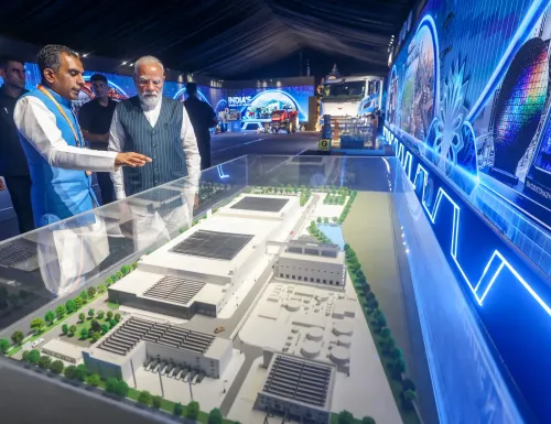
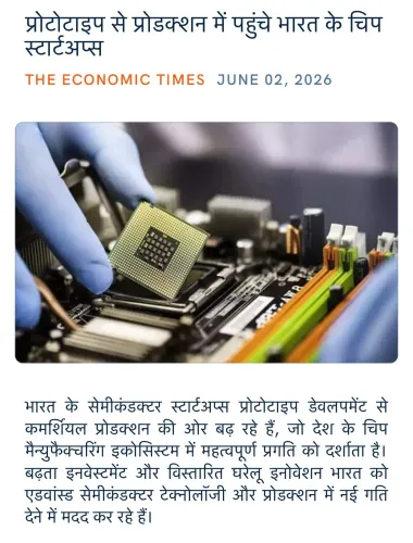
Commercial chip-packaging production has begun at India's third semiconductor plant , as announced on 4 July 2026 .
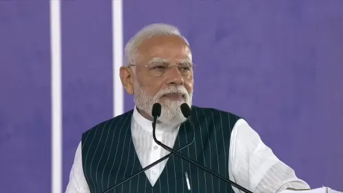
Prime Minister Narendra Modi addressed the inauguration, framing the launch as fulfilment of a five-year-old national pledge to build a semiconductor hub.
The milestone is anchored in the India Semiconductor Mission , approved in December 2021 with a ₹76,000 crore outlay.
India's strategy combines 'Design in India' and 'Make in India' to develop end-to-end domestic semiconductor capabilities.
The PLI scheme for IT hardware , expanded in 2023 , provides capital subsidies supporting semiconductor assembly and packaging units.
Focus now shifts to capacity utilisation and potential new incentives to advance India toward full-scale chip fabrication .
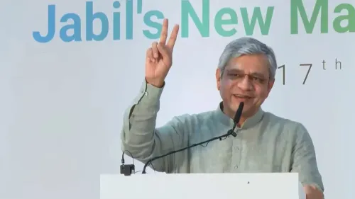
Union Jal Shakti Minister C. R. Paatil on Saturday, 4 July 2026, shared a statement by Prime Minister Narendra Modi marking the commencement of commercial chip-packaging production at India's third semiconductor plant, calling the milestone proof that India delivers on its commitments. The post, shared under the hashtag #SemiconHubBharat, quoted the Prime Minister's remarks at the inauguration event.
Context
Paatil's post quotes Prime Minister Modi directly: 'Aaj ka ye karyakram is baat ka praman hai ki Bharat jo than leta hai, wo karke dikhata hai' — 'Today's programme is proof that when India resolves to do something, it delivers.' Modi noted that five years ago India had pledged to become a semiconductor hub, and that the country has moved forward under the twin mantras of 'Design in India' and 'Make in India'. The launch of commercial chip-packaging production at the third plant is presented as the latest fulfilment of that pledge.
Policy Backdrop
India's semiconductor ambitions are anchored in the India Semiconductor Mission (ISM), approved in December 2021 with a budgetary outlay of ₹76,000 crore, designed to build domestic capabilities in chip design, assembly, testing, and packaging. The mission sits within the broader Atmanirbhar Bharat framework, which seeks to reduce dependence on concentrated East Asian supply chains. The Make in India programme, launched in September 2014, laid the earlier groundwork by positioning India as a global manufacturing destination across sectors including electronics. A subsequent expansion of the Production Linked Incentive (PLI) scheme for IT hardware in 2023 further extended support to semiconductor assembly and packaging units, providing capital subsidies to attract investment.
Stakeholders and Impact
The commissioning of a third commercial chip-packaging facility is significant for semiconductor manufacturers and electronics exporters who have been watching India's execution record closely before committing deeper capital. Each operational plant strengthens India's credibility as an alternative node in the global semiconductor supply chain, a case the government has been making to international chipmakers since the global shortage of 2021-22 exposed the risks of geographic concentration. Domestic electronics assemblers stand to benefit from shorter, more reliable component supply lines as packaging capacity grows inside the country.
What's Next
Attention will now turn to capacity utilisation rates at all three commissioned plants and whether the government announces fresh incentives in upcoming budgets to accelerate progress toward full-scale fabrication — widely regarded as the more complex and capital-intensive frontier of semiconductor self-reliance. The pace at which approved units under the India Semiconductor Mission reach commercial scale will be a key indicator of whether India's #SemiconHubBharat ambition translates into durable industrial capacity. Policymakers are also expected to outline a roadmap for moving beyond packaging toward advanced chip design and wafer fabrication in the medium term.
Point of View
If incremental, step in India's decade-long effort to convert policy ambition into industrial reality. That a minister from the Jal Shakti portfolio amplified the message underscores how semiconductor self-reliance has become a whole-of-government political narrative, not merely a technology-ministry talking point. The framing of a 'five-year resolve' ties the milestone directly to the 2021 India Semiconductor Mission approval, giving the BJP a concrete deliverable to campaign on ahead of electoral cycles. The harder test — moving from packaging to advanced fabrication — remains ahead, and the government's ability to sustain subsidy commitments and attract global chipmakers will determine whether the hub ambition holds.
NationPress
4 Jul 2026
Frequently Asked Questions
What is India's third semiconductor plant and where is it located?
India's third semiconductor plant to commence commercial chip-packaging production was referenced in Prime Minister Modi's remarks on 4 July 2026. The exact identity and location of the facility have not been officially specified in available public records at the time of reporting.
What is the India Semiconductor Mission?
The India Semiconductor Mission is a government programme approved in December 2021 with an outlay of ₹76,000 crore to build domestic capabilities in chip design, assembly, testing, and packaging as part of the Atmanirbhar Bharat initiative.
What does chip packaging mean and why does it matter?
Chip packaging is the process of encasing a semiconductor die in a protective casing and connecting it to other components. It is a critical step in the semiconductor supply chain and serves as an accessible entry point for countries building domestic chipmaking capacity before advancing to full fabrication.
What is the 'Design in India' initiative for semiconductors?
'Design in India' is a government push to develop indigenous semiconductor chip design capabilities alongside the manufacturing-focused 'Make in India' programme, aiming to create a full domestic value chain from design through production.
Why is C. R. Paatil, a Jal Shakti Minister, posting about semiconductors?
As a senior BJP leader and Union Cabinet minister, C. R. Paatil regularly amplifies the government's broader policy achievements on social media. His post quotes Prime Minister Modi's remarks and is part of a whole-of-government effort to publicise the semiconductor milestone.