CM Dhami Hails India's Third Semiconductor Plant Milestone
Synopsis
Uttarakhand CM Pushkar Singh Dhami on 4 July 2026 celebrated commercial chip packaging production beginning at India's third semiconductor plant, calling it a historic step toward Atmanirbhar Bharat and crediting PM Modi's five-year semiconductor mission with delivering results.
Key Takeaways
Uttarakhand CM Pushkar Singh Dhami posted on 4 July 2026 praising commercial chip packaging production at India's third semiconductor plant .
He described the development as a historic achievement under the Atmanirbhar Bharat , Make in India , and Design in India frameworks.
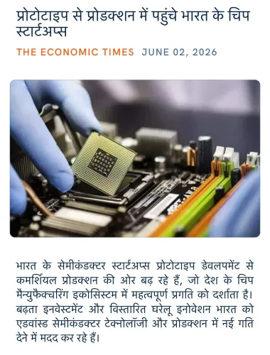
The milestone is rooted in the India Semiconductor Mission , approved in 2021 with an outlay of Rs 76,000 crore .
India's semiconductor strategy prioritises back-end packaging units first, as they are faster to deploy than full wafer fabrication facilities.
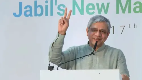
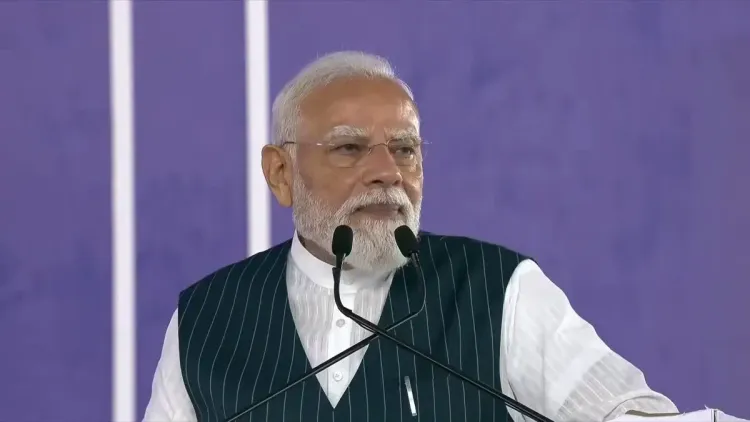
Dhami credited the resolve taken five years ago by PM Narendra Modi as the foundation for the current achievement.
The BJP is positioning each semiconductor milestone as political validation of its long-term manufacturing vision under #SemiconHubBharat .
Uttarakhand Chief Minister Pushkar Singh Dhami on Saturday, 4 July 2026, praised the commencement of commercial chip packaging production at India's third semiconductor plant, calling it a historic achievement under Prime Minister Narendra Modi's leadership. Dhami linked the milestone to the five-year-old national pledge to make India a global semiconductor hub, invoking the Atmanirbhar Bharat, Make in India, and Design in India missions.
Context
Posting in Hindi on X (formerly Twitter), Dhami wrote: 'देश के तीसरे सेमीकंडक्टर प्लांट में चिप पैकेजिंग का व्यावसायिक उत्पादन प्रारंभ होना आत्मनिर्भर भारत, मेक इन इंडिया और डिज़ाइन इन इंडिया की दिशा में एक ऐतिहासिक उपलब्धि है' — translated: 'The commencement of commercial chip packaging production at the country's third semiconductor plant is a historic achievement in the direction of Atmanirbhar Bharat, Make in India, and Design in India.' He credited PM Modi's 'able leadership' for converting a resolve taken five years ago into tangible reality, using the hashtag #SemiconHubBharat.
Policy Backdrop
The milestone sits squarely within the India Semiconductor Mission (ISM), approved by the Union Cabinet in 2021 with an outlay of Rs 76,000 crore to build a full domestic semiconductor ecosystem covering fabrication, assembly, testing, and packaging. The mission was designed to reduce India's near-total dependence on chip imports and integrate the country into global supply chains long dominated by East Asia.
Back-end packaging units were prioritised in the early phases of the mission because they are quicker to deploy than full wafer fabrication facilities. Projects cleared from 2022 onwards under the ISM framework included assembly and packaging facilities across multiple states, with a uniform central incentive structure underpinning each approval.
The broader push aligns with two flagship programmes: Make in India, launched in 2014 and later extended to cover the electronics and semiconductor value chain, and Atmanirbhar Bharat, the self-reliance drive launched in 2020 that explicitly identified semiconductor manufacturing as a strategic priority.
Stakeholders and Impact
The commercial production milestone directly affects domestic electronics manufacturers who currently source packaged chips almost entirely from overseas suppliers, raising costs and creating supply-chain vulnerabilities. A functioning domestic packaging line reduces lead times and foreign-exchange outflows, while generating skilled employment in semiconductor-adjacent trades.
State governments competing to host ISM-approved units stand to gain industrial investment and ancillary economic activity. Global semiconductor firms evaluating India as a diversification destination will watch the ramp-up of existing plants as a signal of execution capability before committing to more capital-intensive front-end fabrication projects.
What's Next
Attention will now turn to production ramp timelines at the three operational or near-operational packaging units and to the next round of India Semiconductor Mission evaluations, which could clear additional fabrication or advanced packaging proposals. The government's stated ambition moves progressively from packaging toward full wafer fabrication — a far more complex and capital-intensive undertaking that will test the durability of the current policy framework.
Dhami's post signals that the BJP intends to keep semiconductor self-reliance prominent in its political messaging, framing each production milestone as validation of the five-year-old national vision articulated by PM Modi.
Point of View
Making even back-end packaging capacity a genuine structural shift. However, the leap from packaging to full-scale wafer fabrication remains the harder test, and the government's ability to deliver on that front will determine whether the 'global hub' narrative holds. For now, each production milestone strengthens the policy arc from the 2021 ISM approval to a credible domestic semiconductor ecosystem.
NationPress
4 Jul 2026
Frequently Asked Questions
What is India's third semiconductor plant and where is it located?
India's third semiconductor plant refers to one of the facilities approved under the India Semiconductor Mission. The specific location of the third plant has not been confirmed in official statements covered here; multiple ISM-approved projects are spread across states including Gujarat.
What is the India Semiconductor Mission?
The India Semiconductor Mission is a central government scheme approved in 2021 with an outlay of Rs 76,000 crore to build a domestic semiconductor ecosystem covering fabrication, assembly, testing, and packaging of chips.
What does chip packaging mean and why does it matter for India?
Chip packaging is the back-end process of encasing a semiconductor die in a protective casing and connecting it for use in electronics. For India, domestic packaging capacity reduces import dependence, cuts costs for electronics manufacturers, and is a stepping stone toward full wafer fabrication.
How does this semiconductor milestone relate to Atmanirbhar Bharat?
Atmanirbhar Bharat, launched in 2020, explicitly includes semiconductor manufacturing as a strategic priority for self-reliance. Commercial chip packaging production at a domestic plant directly advances that goal by reducing India's near-total dependence on imported chips.
What did CM Dhami say about India's semiconductor progress?
CM Pushkar Singh Dhami said on 4 July 2026 that the commencement of commercial chip packaging at India's third semiconductor plant is a historic achievement in the direction of Atmanirbhar Bharat, Make in India, and Design in India, and credited PM Modi's leadership for fulfilling a five-year-old national resolve.