MP CM Office: Youth Driving India's Chip Design, Security
Synopsis
The Chief Minister's Office of Madhya Pradesh amplified India's youth-driven technology narrative on 13 June 2026, linking national security and semiconductor chip design under the Atmanirbhar Bharat policy arc — signalling state-level alignment with central STEM and defence-technology priorities.
Key Takeaways
The Chief Minister's Office of Madhya Pradesh posted on 13 June 2026 connecting India's youth to national security and chip design.
The message aligns with the Atmanirbhar Bharat Abhiyan , launched in 2020 , which prioritises domestic capabilities in defence and electronics.
The India Semiconductor Mission , approved in 2021 , is the central policy vehicle for building a chip design and fabrication ecosystem in India.
The National Education Policy 2020 introduced STEM reforms aimed at creating the youth talent pipeline for these sectors.
State governments amplifying this message signals growing alignment between Madhya Pradesh 's education and skilling agenda and national technology sovereignty goals.
Key indicators to watch include semiconductor unit commissioning timelines and new youth-focused design fellowships from the Ministry of Electronics and IT .
The Chief Minister's Office of Madhya Pradesh on Saturday, 13 June 2026 shared a message highlighting the growing role of India's youth in shaping the country's future — spanning domains from national security to chip design — in a post on X that amplifies the national narrative around India's demographic dividend and technological self-reliance.
Context
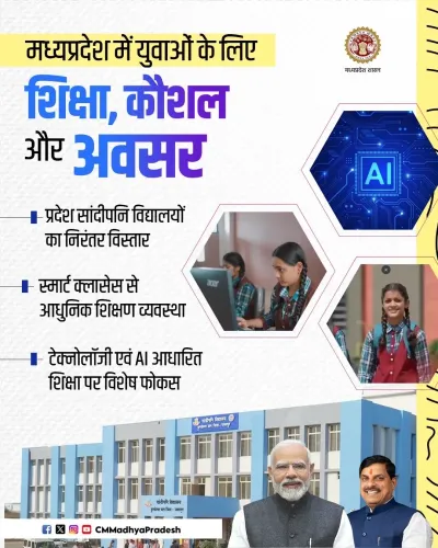
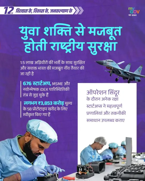
The post, shared by the official Chief Minister's Office of Madhya Pradesh account, states: 'Rashtriya suraksha se lekar chip design tak, yuva shakti Bharat ke bhavishy ko nayi disha de rahi hai' — 'From national security to chip design, the power of youth is giving a new direction to India's future.' The message is accompanied by two images, underscoring the visual emphasis on young Indians at the frontier of strategic and technological work.
The framing connects two otherwise distinct policy domains — defence and semiconductor electronics — under a single youth-centric narrative. This rhetorical bridge has become a recurring feature in official communications from both central and state governments as India positions its young population as a strategic asset.
Policy Backdrop
The post draws on a well-established policy lineage. The Atmanirbhar Bharat Abhiyan, launched in 2020, set the foundational goal of building domestic capabilities in defence manufacturing and electronics, reducing reliance on imports in sectors considered critical to national sovereignty.
The India Semiconductor Mission, approved in 2021, operationalised this ambition specifically for chip design and fabrication by creating a dedicated ecosystem for semiconductor development within India. Simultaneously, the National Education Policy 2020 introduced structural reforms aimed at expanding STEM skills and nurturing innovation among Indian youth — the pipeline that feeds both defence and technology sectors.
Successive governments have consistently framed India's large youth population — often described as a 'demographic dividend' — not merely as an economic resource but as a lever for reducing external dependence in technologies with dual civilian and military applications.
Stakeholders and Impact
The primary stakeholders in this narrative are young Indian engineers and technologists, particularly those entering semiconductor design and defence-technology roles. Firms operating under the India Semiconductor Mission's approved units stand to benefit from a policy environment that ties youth skilling directly to industrial and strategic outcomes.
State governments, including Madhya Pradesh, play a supporting role by amplifying central policy messaging and, in some cases, aligning their own skilling and higher-education programmes with national technology priorities. The Chief Minister's Office sharing this message signals the state's alignment with the broader Atmanirbhar technology agenda.
For young engineers in Madhya Pradesh and across India, the convergence of national security and chip design as career domains reflects a deliberate policy signal: that high-value, sovereign-critical work is being opened up to domestic talent rather than outsourced or imported.
What's Next
Observers tracking this space will watch for commissioning timelines of semiconductor fabrication and packaging units approved under the India Semiconductor Mission, as well as any new youth-focused chip-design fellowships or defence-technology internship programmes announced by the Ministry of Electronics and Information Technology.
As state governments increasingly echo central technology messaging, the next step will likely be concrete state-level initiatives — skilling programmes, innovation hubs, or industry partnerships — that translate this aspirational framing into tangible opportunities for young people in states like Madhya Pradesh.
Point of View
Which carries significant implications for how skilling budgets and industrial policy are justified politically. For state governments, amplifying this narrative costs nothing and signals alignment with New Delhi's priorities — but the real test will be whether state-level programmes, particularly in Madhya Pradesh, translate the message into funded, accessible opportunities for young engineers. The broader pattern suggests India is building a policy consensus around youth-led technology sovereignty that crosses party and administrative lines, making it a durable arc rather than a passing campaign.
NationPress
13 Sept 2026
Frequently Asked Questions
What did the Madhya Pradesh Chief Minister's Office post about on 13 June 2026?
The Chief Minister's Office of Madhya Pradesh posted a message stating that India's youth power is giving a new direction to the country's future, spanning from national security to chip design — amplifying the Atmanirbhar Bharat technology narrative.
What is the India Semiconductor Mission?
The India Semiconductor Mission is a central government programme approved in 2021 to develop a domestic ecosystem for semiconductor chip design, fabrication, and packaging, positioning India as a global hub in this strategic sector.
How does Atmanirbhar Bharat relate to chip design and national security?
The Atmanirbhar Bharat Abhiyan, launched in 2020, set the policy goal of building domestic capabilities in both defence manufacturing and electronics, directly linking chip design and national security as areas where India must reduce external dependence.
Why is Madhya Pradesh sharing messages about chip design and national security?
State governments, including Madhya Pradesh, routinely amplify central government technology and self-reliance messaging to signal policy alignment and to contextualise their own skilling and higher-education programmes within the national agenda.
What role does India's youth play in the country's semiconductor ambitions?
Indian youth, particularly engineering graduates, form the primary talent pipeline for chip design and defence-technology roles. Policies like the National Education Policy 2020 were specifically designed to expand STEM skills among young Indians to support these strategic sectors.