Is the Centre Really Advancing India's Semiconductor Industry with 24 Sanctioned Chip Design Projects?

Synopsis
The Indian government has just approved 24 projects to enhance chip design across various sectors, including surveillance and IoT. This bold move marks a significant step towards strengthening India's semiconductor ecosystem and fostering innovation, positioning the country as a global player. Discover how this initiative is shaping India's technological future.
Key Takeaways
24 chip design projects sanctioned under DLI scheme.
95 companies now have access to advanced EDA tools.
Projects cover sectors like video surveillance and drone detection .
Focus on building a self-reliant semiconductor ecosystem.
Investment of Rs 76,000 crore for semiconductor initiatives.
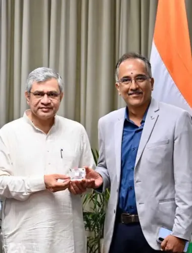
New Delhi, Jan 4 (NationPress) A total of 24 chip design initiatives have been approved in various domains including video surveillance, drone detection, energy meters, microprocessors, satellite communications, and broadband and IoT Systems-on-Chip (SoCs) under the government’s Design Linked Incentive Scheme (DLI), as per an official announcement made on Sunday.
Moreover, 95 firms have gained access to industry-grade Electronic Design Automation (EDA) tools, which significantly cut down design and infrastructure expenses for Indian chip design startups.
The design of semiconductor chips is a crucial value driver in the supply chain, contributing up to 50% of value addition and 30–35% of global semiconductor sales through the fabless segment.
Projects supported by DLI are progressing swiftly, with 16 tape-outs, 6 ASIC chips, 10 patents, over 1,000 engineers engaged, and more than 3× private investment being utilized, as stated.
The Design Linked Incentive (DLI) Scheme, with an allocation of Rs 76,000 crore, is being executed by the Ministry of Electronics and Information Technology (MeitY). This initiative encourages investments in semiconductor and display manufacturing as well as the design ecosystem, providing comprehensive support for design, fabrication, and productization. The C-DAC, a leading R&D organization under MeitY, oversees the DLI Scheme as the nodal agency.
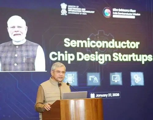
The Semicon India Programme aims to foster a robust, self-sufficient chip design ecosystem by offering financial incentives and access to advanced design infrastructure for local startups and MSMEs.
This scheme is facilitating the shift from design validation to productization, allowing startups and MSMEs to advance toward volume manufacturing, system integration, and market deployment. This evolving ecosystem not only fortifies India’s domestic semiconductor capabilities but also establishes the nation as a credible participant in global chip design and innovation, according to the statement.
India’s semiconductor ecosystem is being bolstered through a unified institutional framework that integrates policy leadership, investment support, capacity building, and indigenous technology development. Key programs and agencies provide extensive backing, from incentivizing chip design and manufacturing to developing skilled talent and promoting open-source microprocessor architectures, ensuring India’s progress toward a self-sufficient and globally competitive semiconductor design ecosystem.
The Chips to Startup (C2S) Programme, currently being implemented, is aimed at academic institutions nationwide to produce 85,000 industry-ready professionals at the B.Tech, M.Tech, and PhD levels, specializing in semiconductor chip design.
The DLI scheme seeks to address existing challenges in India’s domestic semiconductor design sector, helping Indian companies ascend the semiconductor value chain.
A robust fabless capability is essential; without it, a nation remains reliant on imported core technologies even if electronics are locally manufactured. Therefore, developing a solid fabless ecosystem enables India to control the most critical layer of the value chain, safeguard intellectual property, reduce imports, attract manufacturing, and cultivate long-term technological leadership, as emphasized in the statement.
Point of View
This initiative demonstrates India's commitment to becoming a self-reliant hub for semiconductor design and manufacturing. By investing in local capabilities, the government is not only boosting the economy but also enhancing technological sovereignty. The focus on building a robust ecosystem is commendable and aligns with global trends in semiconductor innovation.
NationPress
20 Jun 2026
Frequently Asked Questions
What is the Design Linked Incentive Scheme?
The Design Linked Incentive Scheme (DLI) is a government initiative aimed at promoting semiconductor design and manufacturing in India by providing financial incentives and support for projects.
How many projects were approved under the DLI scheme?
A total of 24 chip design projects have been approved under the DLI scheme, covering various sectors such as video surveillance and IoT.
What is the significance of semiconductor chip design?
Semiconductor chip design is critical as it contributes significantly to the value addition in the supply chain and plays a vital role in the global semiconductor market.
How does the DLI scheme benefit startups?
The DLI scheme provides startups with access to advanced design infrastructure and industry-grade tools, significantly reducing costs and facilitating innovation.
What are the expected outcomes of the Semicon India Programme?
The Semicon India Programme aims to create a self-reliant chip design ecosystem, enhance local talent, and establish India as a key player in the global semiconductor industry.