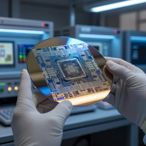
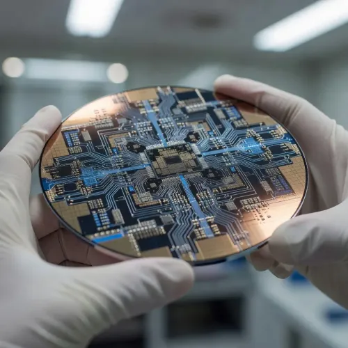
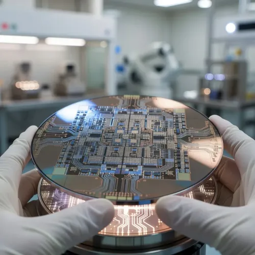
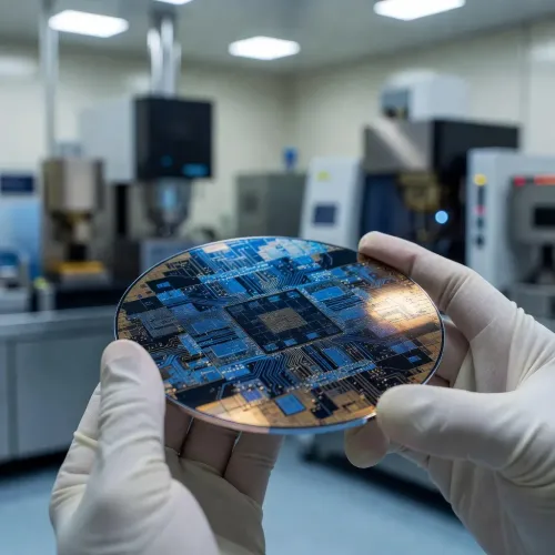
Huawei Tau Scaling Law targets 1.4nm chips by 2031, bypassing EUV
Synopsis
Huawei's newly unveiled Tau Scaling Law claims to deliver 1.4nm-equivalent chip density by 2031 without EUV lithography — a potential 'DeepSeek moment' for hardware that could blunt the strategic force of US semiconductor export controls on China.
Key Takeaways
Huawei Technologies introduced the Tau (τ) Scaling Law on Monday, 26 May 2026 , targeting transistor density equivalent to a 1.4-nanometre chip process by 2031 .
He Tingbo , chairwoman of the Huawei Scientist Committee , said advanced EUV lithography tools will not be required to achieve these nodes.
Gary Ng , senior economist at Natixis Corporate and Investment Bank , warned the law still needs to be 'tested in practice' before its impact can be assessed.
Current US -led export controls block China from accessing EUV machines needed for 3nm nodes and below, making the architectural workaround strategically significant.
The development targets performance gains in both smartphone chips and AI computing systems, with potential consequences for Nvidia 's market position.
Huawei Technologies has unveiled a chip architectural breakthrough it calls the Tau (τ) Scaling Law, a method the company says will enable it to achieve transistor density equivalent to a 1.4-nanometre process in high-end chips by 2031 — without relying on the advanced lithography equipment that US-led export controls have placed out of reach for China.
What Huawei announced
The Shenzhen-based tech giant made the announcement on Monday, 26 May 2026, drawing immediate comparisons to the disruptive impact of DeepSeek's emergence in the artificial intelligence space. He Tingbo, chairwoman of the Huawei Scientist Committee and president of its semiconductor business department, stated that cutting-edge extreme ultraviolet (EUV) lithography tools would no longer be necessary to achieve these advanced nodes — a direct architectural workaround to one of the most consequential technology blockades in modern industrial history.
Why it matters
US-led sanctions currently bar China's semiconductor industry from accessing the most advanced chipmaking technologies, particularly EUV lithography machines required for 3nm nodes and below. If the Tau Scaling Law performs as claimed, it would significantly narrow the gap between Huawei and global semiconductor leaders operating at the cutting edge of chip development.
Gary Ng, senior economist at Natixis Corporate and Investment Bank, said the development signals a shift in the balance of technological leverage: 'The US will have less leverage over export control as China becomes more self-sufficient.' He cautioned, however, that the law still needed to be 'tested in practice.'
The competitive backdrop
Huawei is targeting significant performance improvements in both smartphone chips and AI computing systems through the new scaling law. The announcement arrives as Washington continues to tighten restrictions on advanced chip exports to China, and as domestic Chinese chipmakers have accelerated investment in alternative process architectures. The move draws parallels with DeepSeek's approach of achieving frontier-level AI performance through software and architectural efficiency rather than raw hardware superiority.
Geopolitical implications
Analysts note that Beijing now has a potentially powerful new card to play in its ongoing technology standoff with Washington. A verified path to sub-2nm equivalent performance — achieved without Western equipment — would materially weaken the strategic rationale behind the current export-control architecture. The development has drawn attention from industry observers tracking China's semiconductor self-sufficiency drive, which has been a central pillar of Communist Party industrial policy.
What's next
The critical near-term question is whether the Tau Scaling Law can be validated at production scale. Independent verification by industry analysts — including those at firms such as Bernstein and Omdia — will be closely watched. Should the law prove out in manufacturing, the implications for Nvidia's dominance in AI accelerator chips sold to non-restricted markets, and for the broader US chip-export regime, could be substantial. The 2031 target date gives Huawei five years to translate architectural theory into silicon reality.
Point of View
It systematically dismantles the logic underpinning the US export-control regime, which rests on the assumption that EUV denial creates an insurmountable hardware ceiling for China. The DeepSeek parallel is instructive — both episodes demonstrate Beijing's consistent strategy of routing around Western chokepoints through architectural innovation rather than frontal competition. What mainstream coverage underweights is the signalling function: even an unverified claim at this scale forces Washington to reassess the durability of its sanctions architecture and may accelerate allied countries' hedging behaviour. The five-year window to 2031 is long enough for the geopolitical landscape to shift dramatically, but short enough to sharpen procurement decisions at every major AI data-centre operator today.
NationPress
11 Oct 2026
Frequently Asked Questions
What is Huawei's Tau Scaling Law?
The Tau (τ) Scaling Law is a chip architectural framework unveiled by Huawei Technologies on 26 May 2026 that the company says will enable transistor density equivalent to a 1.4-nanometre process by 2031. Crucially, Huawei claims this can be achieved without EUV lithography machines, which are currently blocked from export to China under US-led sanctions.
Why does Huawei's chip breakthrough matter for US-China relations?
If validated, the Tau Scaling Law would reduce China's dependence on Western chipmaking equipment, weakening a key pillar of US technology export controls. Gary Ng of Natixis Corporate and Investment Bank said 'the US will have less leverage over export control as China becomes more self-sufficient,' though he cautioned the law still needs real-world testing.
How does this compare to the DeepSeek moment?
Like DeepSeek's AI efficiency breakthrough, Huawei's announcement represents an attempt to achieve frontier-level performance through architectural innovation rather than access to the most advanced hardware. Both episodes highlight China's strategy of bypassing Western technology chokepoints rather than competing directly on controlled inputs.
What are EUV lithography machines and why do they matter?
Extreme ultraviolet (EUV) lithography machines are essential tools for manufacturing chips at 3nm nodes and below — the frontier of semiconductor performance. US-led export controls block China from obtaining these machines, making any credible alternative path to advanced node production strategically significant for Beijing's semiconductor ambitions.
Who is most affected if Huawei's 1.4nm claim proves out?
The companies and governments most exposed include Nvidia, whose AI accelerator dominance partly rests on China's inability to produce competitive alternatives, and US policymakers whose export-control strategy depends on maintaining a hardware performance gap. Allied chipmakers and equipment suppliers would also face pressure to reassess their competitive positioning ahead of 2031.