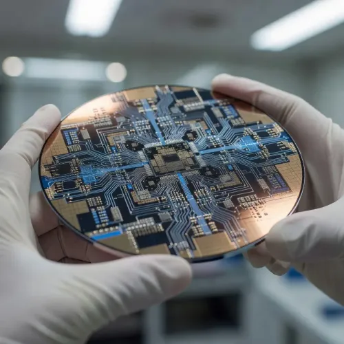
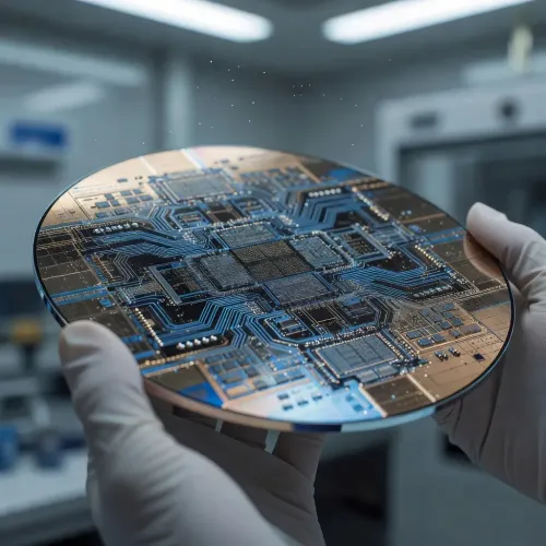
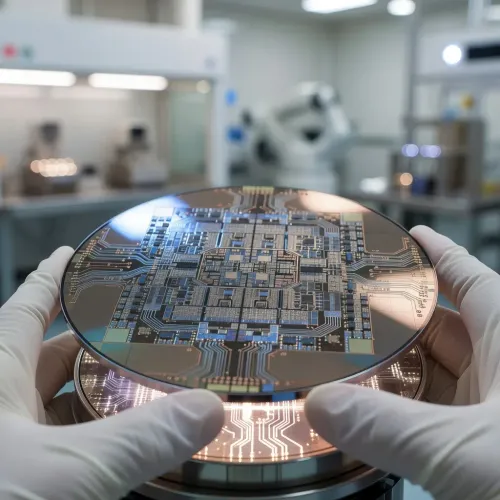
Huawei's Tau Scaling Law targets 1.4 nm chip density by 2031
Synopsis
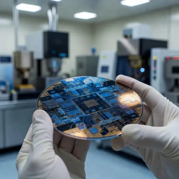
Huawei has unveiled the Tau Scaling Law and LogicFolding architecture, claiming it can achieve 1.4 nm-equivalent transistor density by 2031 — without access to advanced lithography — potentially rewriting the rules of the US-China chip war.
Key Takeaways
Huawei Technologies unveiled the Tau (τ) Scaling Law at the 2026 IEEE ISCAS symposium in Shanghai on 25 May 2026 .
The law, presented by He Tingbo , replaces traditional geometric transistor miniaturisation with time (τ) scaling, earning the informal name 'Her's Law' .
Huawei claims it has used the Tau Scaling Law to design and mass-produce 381 chips over the past six years .
The companion LogicFolding architecture reduces resistive and capacitive signal load to boost transistor density without advanced lithography nodes.
New Kirin chips launching later in 2026 will be the first to adopt LogicFolding , targeting 1.4 nm -equivalent density by 2031 .
The roadmap directly challenges rivals Nvidia and Advanced Micro Devices in the AI accelerator market amid ongoing US export restrictions .
Huawei Technologies has unveiled a new semiconductor scaling principle and chip architecture it says will deliver transistor density equivalent to a 1.4 nanometre process node by 2031, marking a significant push by the Chinese tech giant to build a self-reliant chip ecosystem independent of Western fabrication technology.
The Tau Scaling Law explained
The new principle, called the Tau (τ) Scaling Law, was presented by He Tingbo, chair of the Huawei Scientist Committee and president of the company's semiconductor business department, during a keynote at the 2026 IEEE International Symposium on Circuits and Systems (ISCAS) held in Shanghai on Monday, 25 May 2026. Informally dubbed 'Her's Law' by peers, the principle proposes replacing traditional geometric transistor miniaturisation with time (τ) scaling — a fundamental departure from the path set by Moore's Law.
According to He Tingbo, the Tau Scaling Law is a new principle guiding "evolution of both semiconductors and electronic systems." Huawei claims it has already applied this law to design and mass-produce 381 chips over the past six years.
LogicFolding architecture: the enabling technology
Alongside the scaling law, He introduced LogicFolding, a core chip architecture that reduces resistive and capacitive load in signal propagation, ultimately boosting transistor density without relying on leading-edge lithography. The company said its upcoming Kirin chips, scheduled to launch later in 2026, will be the first to adopt the LogicFolding architecture and are expected to deliver enhanced chip performance as a result.
Why it matters
Huawei has been cut off from advanced chipmaking equipment — including extreme ultraviolet (EUV) lithography machines — following US export restrictions that have effectively blocked access to sub-7 nm fabrication from foundries such as TSMC. By developing an architecture that achieves equivalent transistor density through system-level innovation rather than process node shrinks, Huawei is attempting to sidestep the hardware blockade entirely.
The roadmap puts Huawei on a trajectory that, if realised, would place its chips in competitive proximity to the most advanced nodes being developed by global peers, with direct implications for its Ascend AI chip series that currently competes — under constrained supply — with offerings from Nvidia and Advanced Micro Devices.
The competitive backdrop
The announcement lands at a moment of intensifying competition in AI accelerator hardware. Nvidia and Advanced Micro Devices continue to advance their GPU roadmaps, while US export controls have progressively tightened access to high-end chips for Chinese buyers. Huawei's Ascend series has emerged as the primary domestic alternative, and a credible long-term scaling roadmap strengthens its standing with Chinese cloud providers and AI developers who can no longer source Nvidia hardware freely.
What's next
The immediate milestone to watch is the commercial launch of the new Kirin chips later in 2026, which will serve as the first real-world validation of the LogicFolding architecture. Whether the performance gains translate into competitive benchmarks against leading global chips will determine how seriously the industry treats the 2031 density target. Independent verification of Huawei's claimed transistor density equivalence will be closely scrutinised by analysts and rivals alike.
Point of View
It validates the entire architectural thesis years ahead of the headline milestone. The broader implication is that US chip controls may be accelerating, rather than preventing, indigenous Chinese innovation in semiconductor design — a dynamic that neither Washington nor Silicon Valley has fully priced in. Nvidia and AMD face a competitor that, by 2031, could credibly claim parity on transistor density without ever needing a cutting-edge fab.
NationPress
10 Oct 2026
Frequently Asked Questions
What is Huawei's Tau Scaling Law?
The Tau (τ) Scaling Law is a new semiconductor scaling principle unveiled by Huawei that replaces traditional geometric transistor miniaturisation with time (τ) scaling. Presented by He Tingbo at the 2026 IEEE ISCAS symposium in Shanghai, it is informally called 'Her's Law' and has reportedly guided the design of 381 Huawei chips over six years.
What is Huawei's LogicFolding architecture?
LogicFolding is a chip architecture introduced alongside the Tau Scaling Law that reduces resistive and capacitive load in signal propagation to boost transistor density. Huawei's upcoming Kirin chips, expected later in 2026, will be the first products to use it.
Why is Huawei developing its own chip scaling technology?
US export restrictions have blocked Huawei's access to advanced chipmaking equipment and leading-edge foundry services, preventing it from producing chips at the most advanced process nodes. The Tau Scaling Law and LogicFolding are designed to achieve comparable transistor density through architectural innovation rather than lithography advances.
How does Huawei's 1.4 nm target compare to Nvidia and AMD?
Huawei's roadmap targets transistor density equivalent to a 1.4 nm process node by 2031, a level that would place it in competitive proximity to the most advanced chips from Nvidia and Advanced Micro Devices. The claim remains to be independently verified, with the 2026 Kirin chip launch serving as the first real validation point.
What is the significance of the 2026 Kirin chip launch?
The upcoming Kirin chips, scheduled for later in 2026, are the first commercial products to adopt the LogicFolding architecture and will provide the earliest measurable evidence of whether Huawei's new scaling approach delivers real-world performance gains at scale.