Huawei Kirin 9050 Pro debuts LogicFolding to beat US chip curbs
Synopsis
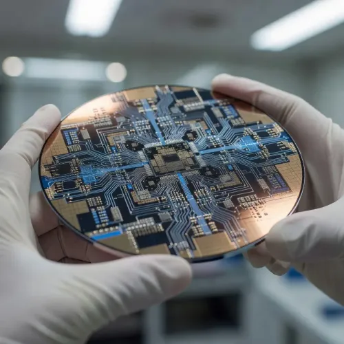
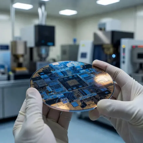
Huawei's Kirin 9050 Pro — the first chip using its LogicFolding architecture — claims a 42% performance leap and represents the company's most ambitious attempt yet to engineer around US export controls by splitting computing functions across two active silicon layers instead of shrinking transistors.
Key Takeaways
Huawei Technologies launched the Kirin 9050 Pro on Monday, September 8, 2026 , the first commercial chip using its LogicFolding architecture.
The chip claims a 42 per cent overall performance improvement over its predecessor, according to the company.
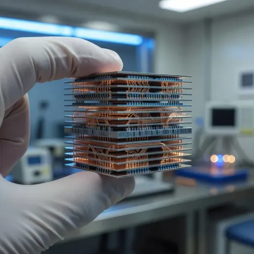
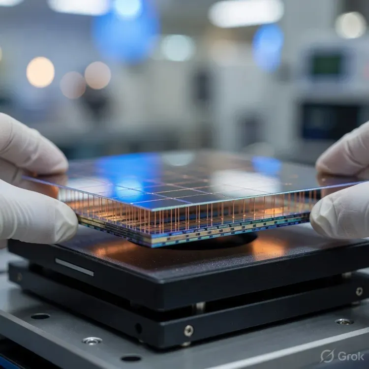
LogicFolding splits core computing functions across two active silicon layers , unlike conventional 3D stacking of self-contained dies.
Leslie Wu , CEO of RHCC , called the architecture 'a compensatory route — a choice born of external constraints,' warning of yield risks from complex wafer thinning and vertical wiring steps.
The Kirin 9050 Pro powers Huawei 's new Mate XT 2 trifold smartphone, serving as the first mass-market test of the new design.
If successful, LogicFolding could be extended to Huawei 's Ascend AI accelerator line, including the anticipated Ascend 950 .
Huawei Technologies launched the Kirin 9050 Pro on Monday, September 8, 2026, marking the first commercial deployment of its proprietary LogicFolding architecture — a high-stakes engineering bet that the Shenzhen-based company can circumvent US export controls by stacking active circuit layers rather than shrinking transistors further. The chip powers the new Mate XT 2 trifold smartphone and, according to the company, delivers a 42 per cent improvement in overall performance over its predecessor alongside better power efficiency.
What LogicFolding Actually Does
Unlike conventional 3D integration techniques that stack largely self-contained dies, Huawei's LogicFolding splits core computing functions across two active silicon layers engineered to operate as a single unified unit. The approach is designed to extract greater computing density from existing semiconductor manufacturing processes — bypassing the need for the world's most advanced lithography equipment, which remains blocked under US export restrictions.
For chipmakers with unrestricted access to leading-edge fabrication tools, 3D stacking is typically a supplementary technique layered on top of transistor miniaturisation. For Huawei, constrained by trade sanctions, it has become the primary architectural strategy.
Why It Matters
Leslie Wu, CEO of semiconductor consultancy RHCC, described the move in a research note as a calculated but costly pivot. 'LogicFolding is first and foremost a compensatory route — a choice born of external constraints,' Wu said. He cautioned that bonding two active silicon layers demands complex manufacturing steps — including precise wafer thinning and microscopic vertical wiring — that can weigh on factory yields.
For global competitors that can simply print smaller transistors on a single layer, the economics of LogicFolding may be less compelling, according to Wu. The yield challenges represent a tangible cost disadvantage that Huawei must manage at scale.
The Competitive Backdrop
Huawei's broader chip ambitions extend well beyond mobile processors. The company's Ascend line of AI accelerators — including the Ascend 910C and the anticipated Ascend 950 — has drawn significant attention across Southeast Asian markets, including Malaysia, as regional buyers seek alternatives to restricted US chips. The LogicFolding architecture, if proven viable at volume, could eventually inform the design of future Ascend AI accelerators.
Industry analysts note that Huawei appears to be developing its own scaling framework — reportedly referencing a Tau Scaling Law and a platform codenamed Somala — as part of its longer-term push to compete in AI compute without access to leading-edge nodes.
What's Next
The Kirin 9050 Pro serves as the first real-world stress test for LogicFolding, with mass-market deployment through the Mate XT 2 providing yield and reliability data at commercial scale. Analysts and supply-chain observers will be watching closely to see whether the architecture can deliver consistent performance without prohibitive manufacturing losses.
If LogicFolding proves manufacturable at competitive yields, Huawei could apply the technique more aggressively to its Ascend AI chip roadmap — a development that would intensify the technology competition with US-aligned semiconductor suppliers across Asia-Pacific.
Point of View
As RHCC's Leslie Wu bluntly notes, a constrained workaround; the real question is whether yield economics can ever make it competitive against a single-layer design printed on a 2nm-class node. The broader pattern here is one of forced architectural divergence: US export controls are not stopping Huawei so much as redirecting its engineering talent into paths that could eventually produce genuinely novel techniques. The sleeper risk that most analysts underweight is the Ascend AI accelerator pipeline — if LogicFolding scales to datacenter silicon, the competitive pressure on US-aligned suppliers in Southeast Asia intensifies considerably.
NationPress
24 Oct 2026
Frequently Asked Questions
What is Huawei's LogicFolding architecture?
LogicFolding is a semiconductor design approach developed by Huawei that splits core computing functions across two active silicon layers engineered to work as a single unit. Unlike conventional 3D stacking, which connects largely self-contained dies, LogicFolding integrates the logic itself across layers to boost performance without requiring advanced lithography equipment blocked by US export controls.
What performance gains does the Kirin 9050 Pro offer?
According to Huawei , the Kirin 9050 Pro delivers a 42 per cent improvement in overall performance compared to its predecessor, alongside improved power efficiency. The chip is the first commercial product to use the LogicFolding architecture and powers the Mate XT 2 trifold smartphone.
Why is Huawei using LogicFolding instead of smaller transistors?
Huawei cannot access the world's most advanced lithography equipment due to US export controls, which block the tools needed to print the smallest transistors. LogicFolding is the company's primary architectural strategy to extract greater computing density from the manufacturing processes it can still access, according to industry analysts.
What are the risks of Huawei's LogicFolding approach?
Leslie Wu , CEO of RHCC , warned that bonding two active silicon layers requires complex steps — including precise wafer thinning and microscopic vertical wiring — that can reduce factory yields. For competitors able to print smaller transistors on a single layer, the economics of LogicFolding may be less attractive, he said in a research note.
Could LogicFolding be used in Huawei's AI chips?
Analysts suggest that if LogicFolding proves viable at commercial scale through the Kirin 9050 Pro , Huawei could apply the architecture to its Ascend AI accelerator line, including the anticipated Ascend 950 . The company has been expanding its Ascend chip presence across Southeast Asian markets, including Malaysia , as a substitute for US -restricted alternatives.