Huawei's Ren Zhengfei backs Tau Scaling Law to survive US chip sanctions

Synopsis
Huawei founder Ren Zhengfei has for the first time publicly endorsed the Tau Scaling Law, calling it the company's only escape route from US chip sanctions — a remarkable admission that survival, not disruption, is driving one of China's boldest semiconductor bets.
Key Takeaways
Ren Zhengfei , 81 , publicly endorsed Huawei 's Tau Scaling Law for the first time, describing it as 'the only path forward to break the siege' imposed by US sanctions.
The Tau Scaling Law was originally unveiled in May 2026 by He Tingbo , president of Huawei 's chip unit HiSilicon .
Ren said tens of thousands of employees spent six years of continuous iteration developing the alternative chip-scaling framework.
Ren 's remarks were posted on Huawei 's internal Xinsheng Community intranet and reported by the state-backed Science and Technology Daily .
The quotes also serve as the preface to a new book on Huawei 's management philosophy by company consultant Tian Tao .
Huawei did not immediately respond to a request for comment on the statements.
Huawei Technologies founder Ren Zhengfei, 81, has publicly endorsed the company's Tau Scaling Law chip-design principle, calling it the sole viable path for the Chinese tech giant to endure escalating US semiconductor sanctions. His remarks, published on Friday, July 25, 2026, were drawn from internal communications posted on Huawei's Xinsheng Community intranet and cited by the state-backed Science and Technology Daily.
Survival, Not Disruption
'The Tau Scaling Law is the only path forward for Huawei to break the siege,' Ren said in the internal remarks. He was explicit that the motivation was existential rather than competitive ambition, framing the architecture as a necessity born of constraint rather than a desire to upend industry norms. Huawei did not immediately respond to a request for comment.
'Other manufacturers have multiple paths to choose from. But for Huawei to escape, survive and thrive, tens of thousands of employees have spent six years of continuous iteration carving out a path that is now maturing,' Ren said. 'It is not to disrupt or replace anything, but simply finding a viable road.'
What Is the Tau Scaling Law?
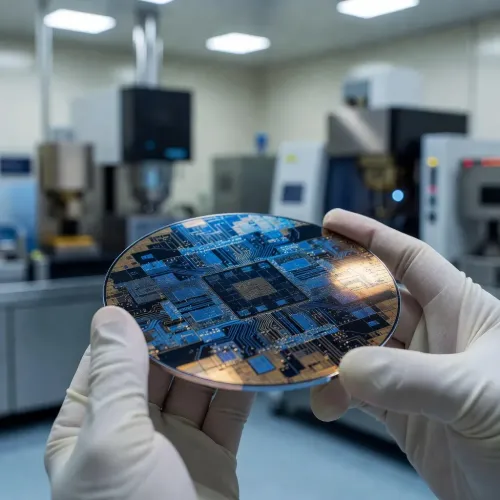
The Tau Scaling Law was first unveiled in May 2026 by He Tingbo, president of Huawei's semiconductor arm HiSilicon. It represents an alternative chip-scaling framework developed internally, reportedly in response to Huawei's inability to access leading-edge EUV lithography equipment and advanced node processes controlled or restricted by US-aligned suppliers. The law is understood to underpin future iterations of Huawei's Kirin chip series and the LogicFolding architecture.
Ren's endorsement marks his first public backing of the framework since He Tingbo's announcement, lending the initiative the full weight of the founder's authority. His quotes also appear as the preface to a new book on Huawei's management philosophy authored by company consultant Tian Tao.
Why It Matters
The statement signals that Huawei's leadership views the Tau Scaling Law not as an experimental detour but as the company's primary long-term semiconductor roadmap. With access to sub-7nm processes effectively blocked and EUV tools off-limits, developing a proprietary scaling law could allow HiSilicon to extract greater performance from domestically available fabrication nodes. The broader implication is that China's semiconductor ecosystem may increasingly bifurcate from global standards set by Moore's Law-driven incumbents.
The Competitive Backdrop
Global chipmakers including those in the US, South Korea, and Taiwan continue to advance along conventional Moore's Law scaling trajectories, with access to EUV and next-generation High-NA EUV tools. Huawei's pivot to an alternative scaling paradigm reflects the asymmetric innovation pressure that sanctions have imposed on Chinese semiconductor developers. The Tau Scaling Law may also influence domestic peers and China's broader chip-design community, which faces similar supply-chain restrictions.
What's Next
Industry observers will watch for concrete benchmarks demonstrating the Tau Scaling Law's real-world performance gains in upcoming Kirin or Mate-series devices. The publication of Tian Tao's management book, prefaced by Ren Zhengfei's endorsement, is also expected to amplify the framework's profile within China's technology policy circles and state media. How quickly HiSilicon can translate the principle into competitive silicon will be the defining test of the strategy.
Point of View
If validated in silicon, could accelerate the decoupling of Chinese chip-design standards from the global Moore's Law consensus — with downstream consequences for every multinational fabless company that still hopes to serve both markets. The state-media amplification via Science and Technology Daily and the People's Daily ecosystem suggests Beijing views the Tau Scaling Law as a policy-aligned narrative, not merely a corporate R&D milestone. Investors and policymakers tracking the chip war should watch whether domestic Chinese foundries formally adopt Tau Scaling Law benchmarks, which would mark a structural, not merely rhetorical, bifurcation.
NationPress
23 Oct 2026
Frequently Asked Questions
What is Huawei's Tau Scaling Law?
The Tau Scaling Law is a proprietary chip-design and scaling framework developed by Huawei's semiconductor arm HiSilicon as an alternative to the conventional Moore's Law trajectory. It was unveiled in May 2026 by HiSilicon president He Tingbo and is intended to extract greater performance from fabrication nodes accessible to Huawei despite US export restrictions on EUV lithography equipment.
Why did Ren Zhengfei endorse the Tau Scaling Law?
Ren Zhengfei endorsed the Tau Scaling Law because he views it as Huawei's only viable path to survive tightening US semiconductor sanctions. He stated that unlike global rivals with multiple technological routes available, Huawei's situation demands a singular, internally developed solution carved out over six years of continuous iteration.
When did Ren Zhengfei make these remarks about the Tau Scaling Law?
Ren Zhengfei's remarks were posted on Huawei's internal Xinsheng Community intranet and reported by the state-backed Science and Technology Daily on Friday, July 25, 2026. This was his first public endorsement of the framework since He Tingbo introduced it in May 2026.
How does the Tau Scaling Law relate to US sanctions on Huawei?
US sanctions have effectively cut Huawei off from advanced EUV lithography tools and leading-edge fabrication nodes, blocking the conventional chip-scaling path used by global competitors. The Tau Scaling Law is Huawei's internal response — a framework designed to improve chip performance within the constraints of domestically accessible manufacturing technology.
What chips will use Huawei's Tau Scaling Law?
The Tau Scaling Law is expected to underpin future generations of Huawei's Kirin chip series and the LogicFolding architecture used in its Mate-series devices. Concrete performance benchmarks from devices built on this framework will be the key indicator of whether the strategy delivers competitive silicon.