How Will 2nm Chip Production in India Enhance National Security, Space Exploration, and the Defence Sector?

Synopsis
India's leap into 2nm chip production marks a pivotal moment in its journey towards technological self-reliance. This significant advancement promises to boost national security, enhance space exploration, and strengthen the defence sector, positioning the country as a key player in the global semiconductor arena.
Key Takeaways
2nm chip technology marks a significant step towards India's technological independence.
Enhanced processing power and efficiency are key advantages of smaller chips.
The India Semiconductor Mission has a substantial budget to support innovation.
Student-led initiatives are contributing to rapid advancements in chip design.
India aims to establish itself as a formidable player in the global semiconductor market.
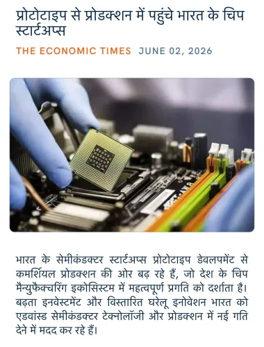
New Delhi, Sep 20 (NationPress) India is evolving from simply assembling devices to engaging in sophisticated design and chip fabrication, with the imminent achievement of 2nm chip production being a significant leap towards technological independence, as stated by the government.
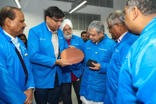
This week, Union Minister Ashwini Vaishnaw inaugurated ARM’s new semiconductor design office in Bengaluru, concentrating on next-generation 2 nanometre chip technology, which is a pivotal advancement in India’s semiconductor journey.
This marks the first instance of a 2 nm chip being designed in India. This cutting-edge technology is set to empower next-generation devices in fields such as AI, mobile computing, and high-performance systems.
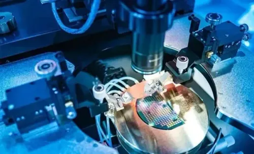
“Thinner chips allow for increased processing capabilities within a compact space, leading to lighter products. Smaller transistors result in enhanced efficiency and lesser power consumption. They hold critical importance for national security, space exploration, and defence applications,” an official statement emphasized.
As per the statement, the total number of approved projects under the India Semiconductor Mission now totals 10 across six states, with a cumulative investment of ₹1.6 lakh crore. The mission itself has a projected budget of ₹76,000 crore to bolster the semiconductor ecosystem.
In May 2025, Vaishnaw inaugurated two cutting-edge semiconductor design facilities in Noida and Bengaluru, marking India’s initial foray into advanced 3-nanometer chip design.
The minister underscored that while India had previously achieved 7 nm and 5 nm designs, attaining 3 nm signifies a new milestone in innovation, paving the way for advancements to 2 nm chip technology.
The global semiconductor sector is expected to reach $1 trillion by 2030, with India's domestic market projected to hit $100–110 billion by the same year.
Domestic startups benefiting from the Design Linked Incentive (DLI) Scheme are expediting chip design processes. At least 23 chip design projects have received approval, and 72 companies are currently utilizing advanced design tools.
Student-led innovation is also on the rise, with 28 chips having been taped out by teams from 25 institutions. Approximately 278 institutions and universities are involved in semiconductor design and research, cultivating a robust talent pool.
This progress fortifies India’s vision of Atmanirbhar Bharat and positions the nation as a frontrunner in the global semiconductor landscape, according to government sources.
Point of View
The push towards 2nm chip technology in India exemplifies a strategic move to enhance self-sufficiency in critical tech sectors. This advancement not only fortifies national security but also propels the nation's ambitions in space exploration and defence. By prioritizing semiconductor manufacturing, India is poised to become a key player in the global technology landscape.
NationPress
1 Jul 2026
Frequently Asked Questions
What is the significance of 2nm chip production in India?
The significance of 2nm chip production in India lies in its potential to boost technological self-reliance, enhance processing capabilities, and support advancements in AI , mobile computing, and national security.
How does smaller chip technology impact efficiency?
Smaller chip technology, such as 2 nm , allows for greater efficiency by enabling more processing power in a compact space, leading to reduced power consumption and lighter products.
What is the India Semiconductor Mission?
The India Semiconductor Mission aims to strengthen the semiconductor ecosystem in India, with a total budget of ₹76,000 crore and numerous approved projects across various states.
How is student innovation affecting chip design in India?
Student innovation is flourishing in India, with various institutions engaged in semiconductor design, resulting in numerous projects and a growing talent pool in the field.
What are the projected growth figures for the semiconductor industry?
The global semiconductor industry is projected to reach $1 trillion by 2030, while India's domestic market is expected to grow to between $100 billion and $110 billion in the same timeframe.