Peking University optical chip system lifts AI inference speed 100x
Synopsis
Peking University researchers have linked standard FPGA chips using a 400 Gbps silicon photonic transceiver, achieving over 100x faster AI inference at one-ninth the compute cost — a potential paradigm shift away from GPU-centric scaling, published in National Science Review on 13 July 2026.
Key Takeaways
Peking University published an all-optical interconnect system for AI distributed inference in National Science Review on 13 July 2026 .
The system delivers more than 100 times faster inference speeds compared to conventional electronic interconnect approaches.
Compute resource consumption is reduced to just one-ninth of typical requirements.
The architecture uses FPGA chips as modular building blocks, connected via a custom silicon photonic transceiver chip running at 400 gigabits per second .
Corresponding authors are Professor Shu Haowen and Professor Wang Xingjun of Peking University .
FPGAs are not subject to current U.S. export controls, making this approach strategically significant for Chinese AI development.
Peking University researchers have developed an all-optical interconnect system that boosts AI distributed inference speeds by more than 100 times while consuming just one-ninth of conventional computational resources, according to a study published in the journal National Science Review on 13 July 2026. The breakthrough offers a fundamentally different answer to the AI industry's surging demand for compute power — one that sidesteps the need for ever-larger GPU clusters and energy-hungry data centres.
What the researchers built
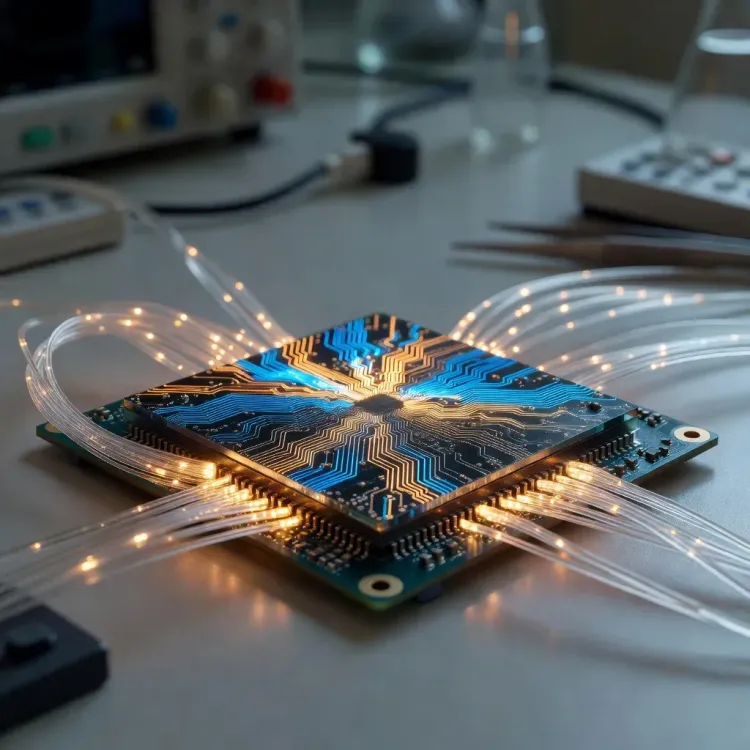
The system uses Field-Programmable Gate Array (FPGA) chips as its core building blocks — programmable devices already deployed in high-stakes parallel-processing environments such as missile guidance systems, autonomous vehicles, and data centres. The team linked these FPGAs optically, rather than through conventional copper-based electrical interconnects, achieving dramatic gains in both speed and efficiency. Two custom-designed communication hardware components serve as the connective tissue. The first is a silicon photonic transceiver chip operating at 400 gigabits per second, which handles the conversion of electrical signals into optical signals and back. The architecture has been described internally as a 'Lego' approach — modular, scalable building blocks that can be assembled to serve different inference workloads.The researchers behind the work
The corresponding authors of the study are Professor Shu Haowen and Professor Wang Xingjun, both affiliated with Peking University. The paper was published in National Science Review, a high-impact Chinese scientific journal, signalling institutional confidence in the findings. The research represents a convergence of silicon photonics and programmable logic — two fields that have individually matured but rarely been co-optimised at this scale for AI inference.Why it matters
The AI industry's dominant response to growing model complexity has been brute-force scaling: more GPUs, more data centre capacity, more energy. This approach carries mounting costs — financial, environmental, and geopolitical, given ongoing restrictions on advanced chip exports to China. An optical interconnect system that slashes compute requirements to one-ninth of the norm while multiplying throughput by over 100 times could meaningfully alter the economics of inference at scale. FPGAs are not subject to the same export controls as cutting-edge GPU accelerators, making this pathway particularly relevant for Chinese AI developers navigating hardware constraints.The competitive backdrop
Globally, the race to reduce AI inference costs is intensifying. Hyperscalers and chip designers alike are investing in custom silicon, optical interconnects, and neuromorphic approaches to escape the power and cost ceiling of GPU-centric architectures. China's semiconductor research community has accelerated its focus on alternative compute paths in response to U.S. export controls, and this study from Peking University is among the most concrete demonstrations of that pivot.What's next
The study's modular 'Lego' design philosophy suggests the system could be scaled or adapted for different AI workloads beyond distributed inference. Whether the architecture can transition from academic demonstration to commercial deployment — and at what cost — will be the critical question for the industry to watch.Point of View
Export controls, and cost inflation are all converging. What mainstream coverage tends to underplay is the strategic dimension: FPGAs sit outside the most sensitive U.S. chip export restriction categories, making an FPGA-based optical compute path a meaningful workaround for Chinese AI labs cut off from frontier Nvidia hardware. If the 100x inference speed claim survives peer scrutiny and real-world replication, it could catalyse a broader industry reassessment of optical interconnects as a first-class compute strategy rather than a niche academic pursuit. The 'Lego' modularity framing is also deliberate — it signals scalability and commercial intent, not just a laboratory proof of concept.
NationPress
12 Oct 2026
Frequently Asked Questions
What did Peking University researchers achieve with their optical chip system?
Researchers at Peking University developed an all-optical interconnect system that boosts AI distributed inference speeds by more than 100 times while using only one-ninth of conventional computational resources. The study was published in the journal National Science Review on 13 July 2026 .
How does the Peking University optical interconnect system work?
The system links FPGA (Field-Programmable Gate Array) chips optically instead of through standard electrical connections. A custom silicon photonic transceiver chip operating at 400 gigabits per second converts electrical signals to optical and back, enabling dramatically faster and more efficient data transfer between chips.
Who are the researchers behind the optical chip AI breakthrough?
The corresponding authors of the study are Professor Shu Haowen and Professor Wang Xingjun , both from Peking University in Beijing, China .
Why does this optical chip breakthrough matter for the AI industry?
The AI industry has relied on adding more GPUs and expanding data centres to meet rising compute demand, which is costly and energy-intensive. A system that achieves over 100x faster inference at one-ninth the compute cost could fundamentally change the economics of running large AI models at scale.
Does this research have implications for China's AI chip restrictions?
FPGAs , the core chips used in this system, are generally not subject to the same U.S. export controls that restrict access to advanced GPU accelerators in China . This makes the optical FPGA-based approach a strategically viable compute path for Chinese AI developers facing hardware supply constraints.