ChipIN Centre onboards 1 lakh+ engineers, 300+ chip designs under Semicon India
Synopsis
India's ChipIN Centre has quietly built the country's largest centralised chip-design user base — over one lakh engineers, four crore hours of tool usage, and 300+ chip designs heading to foundries. Combined with ₹1.64 lakh crore committed under the Semicon India Programme and three facilities already in commercial production, the numbers suggest India's semiconductor push has finally crossed the line from ambition to early execution.
Key Takeaways
The ChipIN Centre has onboarded more than one lakh engineers from over 500 organisations , including 400 academic institutions and 100 startups .
More than 300 chip designs have been developed for fabrication, with over four crore hours of chip-design tool usage recorded.
The DLI Scheme has backed projects spanning video surveillance, drone detection, energy meters, microprocessors, satellite communications, and IoT SoCs.
The Semicon India Programme has approved 12 semiconductor projects across six states , with investment commitments exceeding ₹1.64 lakh crore .
Three semiconductor facilities have already commenced commercial production under the programme.
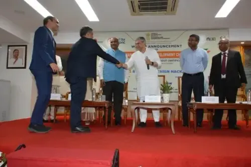
The ChipIN Centre, operating under the Chips to Startup (C2S) Programme and the Design Linked Incentive (DLI) Scheme, has onboarded more than one lakh engineers from over 500 organisations across India — including 400 academic institutions and 100 startups — the Ministry of Electronics and Information Technology (MeitY) announced on 22 September 2026. The milestone, disclosed at SEMICON India 2026 in New Delhi, signals a structural shift in India's ambition to build a homegrown semiconductor design ecosystem.
Scale of the Chip-Design Push
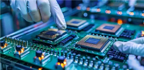
Engineers onboarded through the ChipIN Centre were given access to advanced chip-design tools, fabrication services, and specialised training curricula. Cumulatively, these institutions and startups have developed more than 300 chip designs submitted for fabrication at foundries both within India and abroad.
Tool usage has crossed four crore hours, a figure the IT Ministry describes as creating the largest centralised chip-design user base in the country's history. The scale is unprecedented for a programme that is still in its formative years.
What the C2S Programme and DLI Scheme Cover
The C2S Programme is specifically structured to build semiconductor design capability among students, researchers, and early-stage startups. Its long-term objective is to widen the pool of qualified chip designers and strengthen India's electronic system design capacity at scale.
The DLI Scheme, meanwhile, has backed domestic projects spanning a diverse range of applications — video surveillance, drone detection, energy meters, microprocessors, satellite communications, broadband systems, and Internet of Things (IoT) System-on-Chip (SoC) designs. This breadth reflects the government's intent to embed indigenous chip design across critical and everyday infrastructure.
12 Semiconductor Projects Approved, 3 Already in Production
Under the broader Semicon India Programme, 12 semiconductor projects have received formal approval across six states, with total investment commitments exceeding ₹1.64 lakh crore. Notably, three facilities have already commenced commercial production — a tangible sign that India's semiconductor push has moved beyond policy into execution.
This comes amid intensifying global competition for semiconductor supply chain diversification, with the United States, European Union, Japan, and Taiwan all running parallel incentive programmes. India's timing is deliberate: geopolitical disruptions exposed the vulnerability of concentrating chip production in a single region.
SEMICON India 2026: Ecosystem, Not Just Fabs
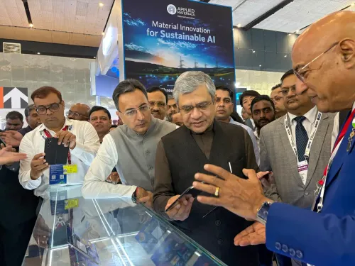
The government used SEMICON India 2026 to emphasise that a competitive semiconductor sector demands far more than chip fabrication alone. The event brought together chip designers, foundries, packaging and testing facilities, equipment and materials suppliers, research institutions, startups, system companies, and workforce developers under one roof.
The emphasis, according to official statements, was on demonstrating capabilities already being built across the value chain — connecting indigenous innovation with global semiconductor market opportunities — rather than outlining aspirational targets alone.
What Comes Next
With three facilities operational and ₹1.64 lakh crore committed across 12 projects, the near-term focus will shift to ramping production yields and attracting global equipment suppliers to set up local operations. Analysts watching the sector note that design capability, while growing rapidly, must eventually connect to domestic fabrication at scale to reduce dependence on overseas foundries. The trajectory over the next two to three years will determine whether India graduates from a chip-design hub to a full-stack semiconductor nation.
Point of View
But the more telling number is four crore hours of chip-design tool usage — that signals sustained, working-level engagement, not just sign-up statistics. The harder question is whether this design talent pipeline will have domestic fabs to feed: with only three facilities in commercial production and most designs still going to overseas foundries, India remains more chip-design hub than chip-making nation. The ₹1.64 lakh crore investment figure also needs scrutiny — committed capital and deployed capital are different things, and semiconductor projects globally have a history of delays and cost overruns. The government is right to showcase momentum at SEMICON India 2026, but the next scorecard must measure yields, not just approvals.
NationPress
22 Sept 2026
Frequently Asked Questions
What is the ChipIN Centre and what has it achieved?
The ChipIN Centre is India's centralised chip-design resource hub operating under the Chips to Startup (C2S) Programme and the Design Linked Incentive (DLI) Scheme. It has onboarded over one lakh engineers from more than 500 organisations, facilitated 300+ chip designs for fabrication, and logged over four crore hours of tool usage — making it the largest centralised chip-design user base in India.
What is the Chips to Startup (C2S) Programme?
The C2S Programme is a government initiative aimed at building semiconductor design capability among students, researchers, academic institutions, and startups across India. Its goal is to create a larger pool of qualified chip designers and strengthen the country's electronic system design ecosystem.
How much has India invested in semiconductor projects under the Semicon India Programme?
The Semicon India Programme has approved 12 semiconductor projects across six states, with total investment commitments exceeding ₹1.64 lakh crore. Three of these facilities have already commenced commercial production as of September 2026.
What kinds of chip designs has the DLI Scheme supported?
The Design Linked Incentive (DLI) Scheme has supported domestic chip-design projects covering video surveillance, drone detection, energy meters, microprocessors, satellite communications, broadband systems, and IoT System-on-Chip (SoC) designs — spanning both national security and consumer infrastructure applications.
What was the significance of SEMICON India 2026?
SEMICON India 2026 was a platform that brought together the full semiconductor value chain — designers, foundries, packaging and testing facilities, equipment suppliers, research institutions, startups, and workforce developers. It was used by the government to demonstrate capabilities already being built across the ecosystem, not merely future targets.