How is CM Majhi Celebrating the Centre's Approval for Semiconductor Units in Odisha?

Synopsis
In a significant milestone for Odisha, CM Majhi has expressed gratitude for the Centre's approval of semiconductor manufacturing units. This move is expected to boost innovation, job creation, and Odisha's role in India's economic vision. Discover how this initiative could transform the state and contribute to national development.
Key Takeaways
Odisha's semiconductor units will foster innovation.
Investment of Rs 4,600 crore will create jobs.
Strategic partnership between state and central government.
Focus on advanced technologies for competitive edge.
Significant applications in various industries.
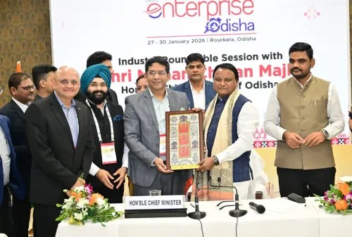
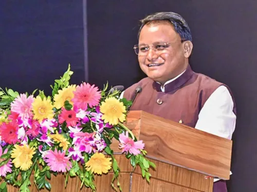
Bhubaneswar, Aug 12 (NationPress) Odisha's Chief Minister Mohan Charan Majhi expressed his heartfelt appreciation to Prime Minister Narendra Modi and Union Railways Minister Ashwini Vaishnaw following the Union Cabinet's endorsement of the establishment of two semiconductor manufacturing facilities in the state.
In a post on his official X account, CM Majhi remarked, "I extend my sincere thanks to Prime Minister @narendramodiji and Union Minister @AshwiniVaishnawji for the Union Cabinet's approval of the two semiconductor manufacturing units in Odisha."
He further noted that the recent revision of the Odisha Semiconductor Manufacturing and Fabless Policy is designed to enhance investment potential, competitiveness, and sustainability. This significant Cabinet approval represents a pivotal moment in the state's industrial and technological progress.
"This collaborative endeavor will boost innovation, create jobs, and fortify Odisha's standing as a crucial contributor to the vision of #AtmanirbharBharat. I anticipate a lasting partnership between the state and Central governments to advance this strategic initiative for the comprehensive development of Odisha and the nation. #doubleengine," stated CM Majhi.
On Tuesday, the Union Cabinet, led by PM Modi, sanctioned four semiconductor projects under the India Semiconductor Mission (ISM).
The approved initiatives include proposals from SiCSem, Continental Device India Private Limited (CDIL), 3D Glass Solutions Inc., and Advanced System in Package (ASIP) Technologies.
According to an official announcement from the Union government, SiCSem and 3D Glass will be established in Odisha, while CDIL will be located in Punjab and ASIP in Andhra Pradesh.
The Union government highlighted that SiCSem Private Limited is partnering with Clas-SiC Wafer Fab Ltd. in the UK to create an integrated facility for Silicon Carbide (SiC)-based Compound Semiconductors in Info Valley, Bhubaneswar, Odisha.
This facility will mark the first commercial compound fabrication in India.
The project aims to produce Silicon Carbide devices.
This compound semiconductor fabrication will boast an annual capacity of 60,000 wafers and a packaging capacity of 96 million units.
The intended products will find applications in missiles, defense equipment, electric vehicles, railways, fast chargers, data center racks, consumer appliances, and solar power inverters.
Conversely, 3D Glass Solutions Inc. plans to establish a vertically integrated advanced packaging and embedded glass substrate unit in Info Valley, Bhubaneswar, Odisha.
This facility will introduce the world's most advanced packaging technology to India.
Advanced packaging will revolutionize efficiency in the semiconductor sector.
The unit will incorporate a wide range of advanced technologies, including glass interposers with passives and silicon bridges, as well as 3D Heterogeneous Integration (3DHI) modules.
The projected capacity for this unit will be approximately 69,600 glass panel substrates, 50 million assembled units, and 13,200 3DHI modules annually.
The products are intended for diverse applications, including defense, high-performance computing, artificial intelligence, radio frequency, automotive, photonics, and co-packaged optics.
These four approved initiatives will establish semiconductor manufacturing facilities with a total investment of roughly Rs 4,600 crore and are expected to create employment opportunities for 2,034 skilled workers, catalyzing the electronic manufacturing ecosystem and indirectly generating numerous jobs.
With these latest approvals, the total number of sanctioned projects under ISM has reached 10, with a cumulative investment nearing Rs 1.60 lakh crore across six states.
Point of View
The approval of semiconductor manufacturing units in Odisha is a significant step towards enhancing India's technological infrastructure. This initiative aligns with the broader goals of self-sufficiency and innovation in the semiconductor sector, fostering economic growth and job creation while ensuring strategic alignment with global trends.
NationPress
14 Jul 2026
Frequently Asked Questions
What is the significance of the semiconductor units in Odisha?
The semiconductor units are pivotal for boosting local industry, creating jobs, and enhancing Odisha's contribution to India's technological landscape.
How many jobs are expected to be created?
The semiconductor projects are anticipated to generate employment for approximately 2,034 skilled professionals.
What is the total investment in the approved projects?
The cumulative investment for the four approved semiconductor projects is around Rs 4,600 crore.
Which companies are involved in the semiconductor projects?
The projects involve SiCSem, Continental Device India Private Limited (CDIL), 3D Glass Solutions Inc., and Advanced System in Package (ASIP) Technologies.
What are the expected applications of the semiconductor products?
The products will have significant applications in various fields, including defense, electric vehicles, consumer appliances, and solar power inverters.