How Will the NaMo Semiconductor Lab Boost India's Chip Design Ecosystem?
Synopsis
The establishment of the NaMo Semiconductor Lab at IIT Bhubaneswar marks a pivotal moment for India's semiconductor industry. This initiative is set to enhance research and training, empowering the youth with critical skills and supporting the nation's ambition to become a leader in chip design and manufacturing.
Key Takeaways
NaMo Semiconductor Lab to be established at IIT Bhubaneswar.
Project funded under MPLAD Scheme with an allocation of Rs 4.95 crore .
Aims to enhance semiconductor skills among India's youth.
Supports Make in India and Design in India initiatives.
Facility expected to boost chip design talent in the country.
New Delhi, Oct 5 (NationPress) In a significant move to enhance India’s semiconductor landscape, Union Minister of Electronics and Information Technology, Ashwini Vaishnaw, has sanctioned the establishment of the ‘NaMo Semiconductor Laboratory’ at IIT Bhubaneswar, as announced by the Ministry of Electronics & IT (MeitY) on Sunday.
This project, estimated at Rs 4.95 crore, will be financed under the MPLAD Scheme.
The NaMo Semiconductor Lab is designed to equip India's youth with industry-ready semiconductor expertise and expand the nation’s burgeoning talent pool in chip design.
“This initiative will position IIT Bhubaneswar as a premier hub for semiconductor research, training, and innovation,” stated the ministry.
“The facility is anticipated to significantly contribute to creating skilled professionals for the forthcoming chip manufacturing and packaging units nationwide,” the ministry further elaborated.
This new laboratory will serve as a vital impetus for the ‘Make in India’ and ‘Design in India’ campaigns by fostering research and innovation in semiconductor design and fabrication.
India currently represents 20 percent of the global chip design talent, with students from 295 universities utilizing advanced EDA tools provided by the industry.
To date, 28 student-designed chips from 20 institutes have been successfully developed at SCL Mohali.
IIT Bhubaneswar was selected for the lab due to its increasing involvement in semiconductor research and existing infrastructure.
Odisha has also recently secured approval for two semiconductor projects under the India Semiconductor Mission—one focusing on an integrated facility for Silicon Carbide (SiC)-based compound semiconductors and another for advanced 3D glass packaging.
The institute already hosts the Silicon Carbide Research and Innovation Centre (SiCRIC), and the new lab will further bolster its cleanroom and R&D capabilities.
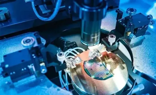
The proposed NaMo Semiconductor Lab will feature essential equipment and software for semiconductor design, training, and fabrication, with Rs 4.6 crore allocated for equipment and Rs 35 lakh for software.
Point of View
The establishment of the NaMo Semiconductor Lab is a commendable initiative that aligns with India's aspirations in the global semiconductor market. This move not only augments our technological capabilities but also empowers the youth, ensuring that India remains a competitive player in chip design and manufacturing.
NationPress
2 Jul 2026
Frequently Asked Questions
What is the NaMo Semiconductor Lab?
The NaMo Semiconductor Lab is a facility established at IIT Bhubaneswar to enhance semiconductor research, training, and innovation in India.
How much funding has been allocated for the lab?
The NaMo Semiconductor Lab has an estimated budget of Rs 4.95 crore, funded under the MPLAD Scheme.
What are the objectives of the NaMo Semiconductor Lab?
The lab aims to empower youth with industry-relevant skills in semiconductor design, supporting the Make in India initiative.
Where is the NaMo Semiconductor Lab located?
The NaMo Semiconductor Lab is located at IIT Bhubaneswar in New Delhi, India.