Bhupender Yadav at Groundbreaking of Amber, Ascent-K Circuits in Gautam Buddha Nagar
Synopsis
Union Environment Minister Bhupender Yadav on 27 June 2026 addressed the groundbreaking ceremony of Amber and Ascent-K Circuits in Gautam Buddha Nagar, Uttar Pradesh, reinforcing India's Atmanirbhar Bharat push for domestic electronics manufacturing in the NCR industrial corridor.
Key Takeaways
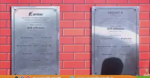
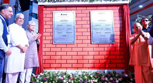
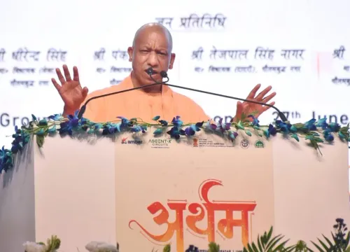
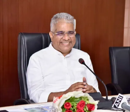
Union Environment Minister Bhupender Yadav addressed the groundbreaking ceremony of Amber and Ascent-K Circuits in Gautam Buddha Nagar on 27 June 2026 .
Gautam Buddha Nagar , encompassing Noida and Greater Noida , is one of northern India's most active electronics manufacturing zones.
The projects align with the Production Linked Incentive (PLI) scheme for electronics notified in 2020 and the India Semiconductor Mission launched in 2021 .
Environment Ministry participation signals early integration of clearance and sustainability planning into industrial project launches.
Uttar Pradesh has been actively courting electronics FDI as part of its industrial corridor development strategy under the Atmanirbhar Bharat framework.
Environmental impact assessments and state-level approvals remain key next steps before full construction commences at both sites.
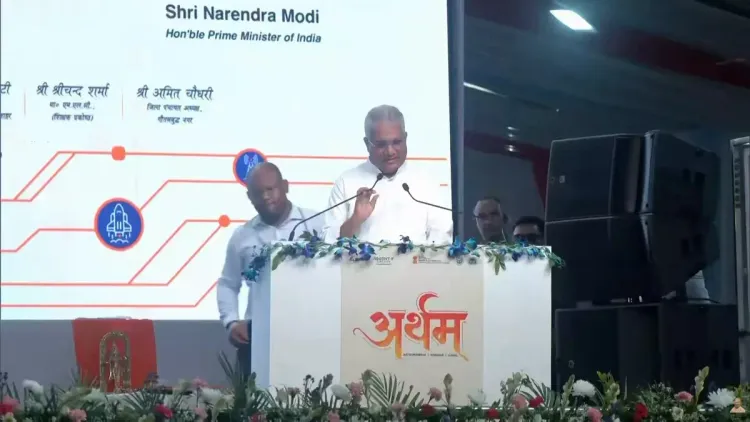
Union Environment Minister Bhupender Yadav addressed the groundbreaking ceremony of Amber and Ascent-K Circuits in Gautam Buddha Nagar, Uttar Pradesh, on Saturday, 27 June 2026, marking a fresh push for electronics manufacturing in the National Capital Region.
Yadav shared his address from the event on social media, writing: 'आज जनपद गौतमबुद्ध नगर में Amber एवं Ascent-K Circuits के Groundbreaking Ceremony में मेरा संबोधन' ('Today, my address at the Groundbreaking Ceremony of Amber and Ascent-K Circuits in Gautam Buddha Nagar district'). The event signals continued momentum in Uttar Pradesh's drive to position itself as a hub for electronics and industrial investment.
Context
Gautam Buddha Nagar — the district encompassing Noida and Greater Noida — has emerged as one of the most active electronics and IT manufacturing zones in northern India. Its proximity to the national capital, established infrastructure, and policy support from both the state and central governments have drawn a steady stream of industrial investment in recent years.
The groundbreaking of two separate circuit-manufacturing units at the same event reflects a broader clustering strategy, where complementary electronics firms are encouraged to set up in the same industrial corridor to share supply-chain and logistics advantages.
Policy Backdrop
The projects fit within India's wider Atmanirbhar Bharat framework, under which the central government has rolled out a series of incentive schemes since 2020 to reduce dependence on imported electronics components. The Production Linked Incentive (PLI) scheme for electronics and IT hardware, notified in 2020, has been a key instrument in attracting domestic and foreign investment into segments such as printed circuit board assembly and semiconductor packaging.
The India Semiconductor Mission, launched in 2021, further expanded the policy architecture by targeting domestic capacity in chips and display manufacturing. Industrial projects in the NCR region increasingly align their investment timelines with these central schemes to access fiscal incentives and expedited clearances.
The Environment Ministry's visible presence at an industrial groundbreaking also underscores a coordinated approach between central ministries — with environment clearances and sustainability norms now being integrated early into project planning rather than treated as a downstream formality.
Stakeholders and Impact
Electronics manufacturers, component suppliers, and logistics firms operating in Uttar Pradesh's industrial corridors stand to benefit from the addition of new circuit-manufacturing capacity in the region. Local employment generation in Gautam Buddha Nagar is a stated objective of such investments, given the district's large semi-skilled and skilled workforce drawn from across the NCR.
State-level industrial bodies and the Uttar Pradesh government, which has actively courted electronics FDI through investor summits, are also key stakeholders. The groundbreaking adds to a visible pipeline of projects the state can cite as outcomes of its investment outreach efforts.
What's Next
Formal environmental impact assessments and state-level regulatory approvals will be critical milestones before construction at both sites can proceed at scale. Observers will also watch for any disbursements or approvals linked to the India Semiconductor Mission or PLI scheme that may be attached to these projects.
As Gautam Buddha Nagar continues to attract electronics investment, the pace of clearances and infrastructure upgrades — power, water, and road connectivity — will determine how quickly the new units can move from groundbreaking to production.
Point of View
Not a friction point. For the BJP, such events serve a dual purpose: demonstrating central-state synergy in Uttar Pradesh, a politically crucial state, while reinforcing the party's economic nationalism narrative ahead of any electoral cycle. The clustering of two electronics firms at a single ceremony in the NCR also reflects a maturing industrial policy logic, where corridor-based co-location is being actively engineered rather than left to market forces. Whether these groundbreakings translate into operational units on schedule will be a key test of how effectively India's incentive architecture converts announcements into production capacity.
NationPress
27 Jun 2026
Frequently Asked Questions
What happened at the Amber and Ascent-K Circuits groundbreaking in Gautam Buddha Nagar?
Union Environment Minister Bhupender Yadav addressed the groundbreaking ceremony of Amber and Ascent-K Circuits in Gautam Buddha Nagar, Uttar Pradesh, on 27 June 2026, marking the formal launch of two new electronics manufacturing projects in the NCR region.
Where is Gautam Buddha Nagar and why is it important for electronics manufacturing?
Gautam Buddha Nagar is a district in Uttar Pradesh within the National Capital Region, encompassing Noida and Greater Noida. Its proximity to Delhi, established infrastructure, and policy support have made it one of northern India's leading electronics and IT manufacturing hubs.
What is the India Semiconductor Mission?
The India Semiconductor Mission was launched in 2021 to build domestic capacity in semiconductor and display manufacturing, offering fiscal incentives and support to attract investment in these strategic sectors.
Why was the Environment Minister present at an industrial groundbreaking?
The Environment Ministry's participation signals a coordinated approach where environmental clearances and sustainability norms are integrated early into industrial project planning, rather than addressed after construction begins.
How does the PLI scheme support electronics projects like these in Uttar Pradesh?
The Production Linked Incentive scheme for electronics and IT hardware, notified in 2020, provides financial incentives linked to incremental production, encouraging firms to set up or expand manufacturing capacity in India and reducing dependence on imported components.