Cabinet Clears Semicon 2.0 With ₹1.27 Lakh Crore Outlay
Synopsis
The Union Cabinet has approved Semicon 2.0 with a ₹1.27 lakh crore outlay, announced by Education Minister Dharmendra Pradhan. The policy spans six pillars — design, materials, fabs, packaging, R&D, and talent — and builds on India's earlier semiconductor mission to attract global chip investment.
Key Takeaways
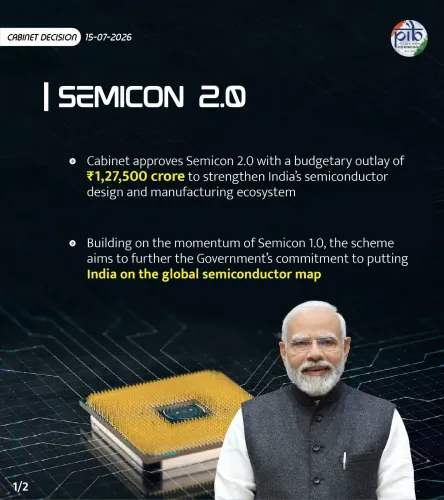
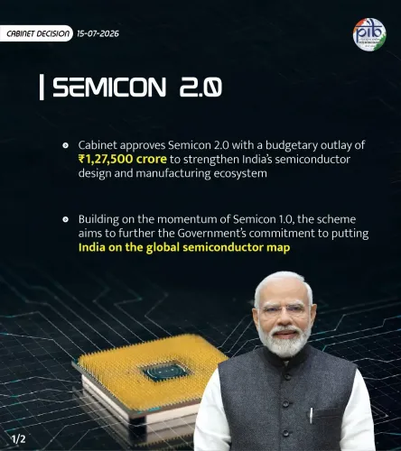
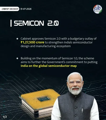
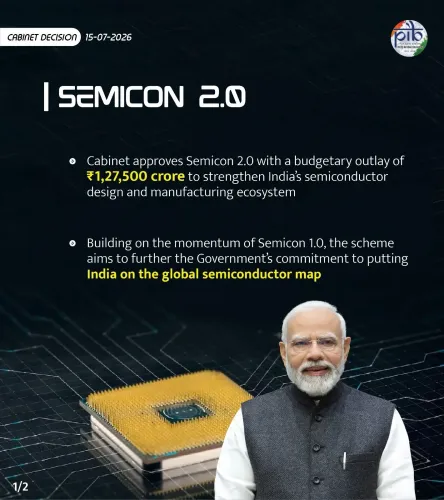
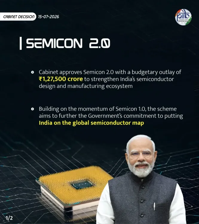
The Union Cabinet has approved Semicon 2.0 with an outlay of ₹1.27 lakh crore , announced on 15 July 2026 .
The policy is built on six pillars : Design, Machines and Materials, Fabs, ATMP/OSAT, R&D, and Talent.
The talent pillar already covers 315 universities and nearly 68,000 trained students .
Semicon 2.0 significantly expands India's earlier ₹76,000 crore India Semiconductor Mission launched in 2021 .
The policy aims to attract global chip investment, strengthen supply chain resilience, and establish India as a trusted semiconductor manufacturing and design hub.
Union Education Minister Dharmendra Pradhan linked the approval directly to Prime Minister Narendra Modi 's Atmanirbhar Bharat and Make in India agenda.
Union Education Minister Dharmendra Pradhan announced on Wednesday, 15 July 2026 that the Union Cabinet has approved Semicon 2.0, a sweeping semiconductor policy package carrying an outlay of ₹1.27 lakh crore, building on the earlier Semicon 1.0 initiative to position India as a global hub for chip design and manufacturing.
Context
Pradhan, posting on X, described the Cabinet decision as a reaffirmation of Prime Minister Narendra Modi's commitment to make India a 'global semiconductor powerhouse.' The announcement comes as India seeks to reduce dependence on imported chips and capitalise on shifting global supply chains accelerated by US-China technology tensions and post-pandemic disruptions.
Semicon 2.0 is structured around six pillars: chip design ecosystem development, machines and materials supply chain, next-generation fabrication (Fabs), advanced chip packaging through ATMP/OSAT facilities, research and development in advanced nodes, and talent development. On the talent front, the minister highlighted that 315 universities and nearly 68,000 students have already been trained under the programme's preceding phase.
Policy Backdrop
India's semiconductor push dates to 2021, when the India Semiconductor Mission (ISM) was launched with an initial outlay of ₹76,000 crore to build a domestic ecosystem spanning manufacturing, design, and packaging. The Make in India programme, launched in 2014, laid the broader industrial policy foundation that semiconductor policy now builds upon.
Production Linked Incentive schemes for IT hardware and the expansion of Electronics Manufacturing Clusters have progressively strengthened the supply-chain infrastructure that Semicon 2.0 now seeks to scale. The new package significantly raises the fiscal commitment, signalling a step-change in ambition from the earlier mission.
Pradhan's role as Education Minister is directly relevant to the talent pillar — universities under the Ministry of Education are central to the trained-workforce pipeline that semiconductor firms require before committing capital to India-based facilities.
Stakeholders and Impact
Global semiconductor firms scouting for geopolitically stable manufacturing and design bases stand to be the primary beneficiaries of the expanded incentive framework. Indian engineering universities and technical institutions are positioned as key delivery partners for the talent component, with the 315-university network already activated under prior phases.
Advanced chip packaging — the ATMP/OSAT segment — is seen as India's nearest-term entry point into the global semiconductor value chain, given lower capital requirements compared to front-end fabrication. Semicon 2.0's explicit pillar for this segment suggests the government intends to accelerate approvals and incentives in this area specifically.
Domestic electronics manufacturers and startups in the chip design space are also likely to benefit from the design ecosystem pillar, which targets scaling India's existing but nascent fabless design industry.
What's Next
Detailed scheme guidelines from the Cabinet notification are expected to specify eligibility criteria, incentive structures, and timelines for each of the six pillars. State governments with existing semiconductor ambitions — including those that have already fielded fab proposals — are likely to move quickly to align their own incentive packages with the central framework.
Memoranda of understanding with global chip companies for design centres and ATMP facilities will be a key metric of early traction. With ₹1.27 lakh crore committed, Semicon 2.0 sets a high bar — and the pace of private investment announcements in the months ahead will determine whether India's semiconductor ambitions translate from policy into production lines.
Point of View
Nearly doubling the fiscal commitment of the original 2021 mission and codifying a structured, multi-pillar approach rather than a single-focus manufacturing subsidy. The explicit inclusion of a talent pillar — and Pradhan's own portfolio as Education Minister — signals that the government is trying to close the workforce gap that has historically deterred advanced semiconductor investment. Framing the announcement around Prime Minister Modi's personal commitment is consistent with the BJP's broader pattern of anchoring flagship industrial policy to the PM's brand. The real test will be whether the outlay translates into ground-broken fabs and signed design-centre agreements before the next electoral cycle.
NationPress
15 Jul 2026
Frequently Asked Questions
What is Semicon 2.0 and what is its budget?
Semicon 2.0 is the Union Cabinet's upgraded semiconductor policy package approved in July 2026 with an outlay of ₹1.27 lakh crore. It builds on Semicon 1.0 and covers six pillars: chip design, machines and materials, fabrication, advanced packaging, R&D, and talent development.
What are the six pillars of Semicon 2.0?
The six pillars are: Design (scaling India's chip design ecosystem), Machines and Materials (supply chain strengthening), Fabs (next-generation manufacturing), ATMP/OSAT (advanced chip packaging), R&D (advanced nodes and emerging technologies), and Talent (315 universities, nearly 68,000 students trained).
Who announced Semicon 2.0 and when?
Union Education Minister Dharmendra Pradhan announced the Cabinet approval of Semicon 2.0 on 15 July 2026 via a post on X, attributing the decision to Prime Minister Narendra Modi's push to make India a global semiconductor powerhouse.
How does Semicon 2.0 differ from India's earlier semiconductor mission?
India's original semiconductor mission was launched in 2021 with a ₹76,000 crore outlay. Semicon 2.0 significantly raises the commitment to ₹1.27 lakh crore and introduces a structured six-pillar framework that explicitly addresses talent, R&D, and supply chain alongside manufacturing incentives.
What is ATMP/OSAT and why does it matter for India?
ATMP (Assembly, Testing, Marking, and Packaging) and OSAT (Outsourced Semiconductor Assembly and Test) refer to the back-end stages of chip production. These require lower capital investment than front-end fabrication, making them India's most accessible near-term entry point into the global semiconductor value chain.