CM Himanta flags Rs 1.25 lakh crore Semiconductor Mission 2.0
Synopsis
Assam Chief Minister Himanta Biswa Sarma on 2 July 2026 shared coverage of India's Semiconductor Mission 2.0, spotlighting a reported Rs 1.25 lakh crore push to build domestic chip manufacturing capacity — a major expansion of the original Rs 76,000 crore mission launched in 2021.
Key Takeaways
CM Himanta Biswa Sarma shared coverage of Semiconductor Mission 2.0 via the NaMo App on 2 July 2026 .
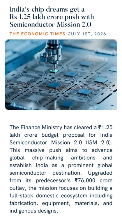
The reported outlay for Semiconductor Mission 2.0 is Rs 1.25 lakh crore , up from the original Rs 76,000 crore approved in December 2021 .
The India Semiconductor Mission is administered by the Ministry of Electronics and Information Technology under the Atmanirbhar Bharat programme.
India seeks to reduce import dependence on chips from Taiwan and China through fiscal incentives and infrastructure support.
Assam is positioning itself as a potential destination for downstream electronics units linked to the national semiconductor drive.
A formal Union Cabinet or Budget announcement is awaited to confirm the expanded outlay and implementation timeline.
Assam Chief Minister Himanta Biswa Sarma on Thursday, 2 July 2026, shared coverage of India's Semiconductor Mission 2.0, highlighting a proposed outlay of Rs 1.25 lakh crore aimed at accelerating the country's chip manufacturing ambitions under the broader Atmanirbhar Bharat framework.
Context
Sarma, who frequently amplifies central government technology and industrial policy from his platform as BJP leader and convenor of the North-East Democratic Alliance (NEDA), shared the article via the NaMo App — a channel routinely used by BJP leaders to circulate policy developments to party workers and the public. The post carries no additional commentary, allowing the headline figure of Rs 1.25 lakh crore to speak for itself.
India's semiconductor push has been building steadily since December 2021, when the Union Cabinet under Prime Minister Narendra Modi approved the original India Semiconductor Mission with an outlay of Rs 76,000 crore. The latest reported expansion — now branded Semiconductor Mission 2.0 — would represent a significant scaling of that commitment.
Policy Backdrop
The India Semiconductor Mission, administered by the Ministry of Electronics and Information Technology, was designed to attract semiconductor fabrication, assembly, testing, marking, and packaging units through fiscal incentives and infrastructure support. The scheme fits within a larger architecture of Production-Linked Incentive (PLI) programmes that successive central budgets have expanded to cover electronics and components.
India's dependence on semiconductor imports — particularly from Taiwan and China — has long been flagged as a strategic vulnerability. Geopolitical disruptions in global chip supply chains during 2020–22 sharpened the policy urgency, prompting the government to combine central fiscal incentives with state-level facilitation to attract global and domestic chipmakers.
Assam itself has positioned itself as a candidate destination for downstream electronics and component manufacturing linked to these national missions, making CM Sarma's amplification of the policy development consistent with the state's industrial outreach strategy.
Stakeholders and Impact
The primary beneficiaries of an expanded semiconductor mission would be electronics manufacturers, global and domestic semiconductor companies eyeing India as a production base, and the broader ecosystem of component suppliers and skilled engineering talent. A Rs 1.25 lakh crore commitment, if confirmed through a formal cabinet or budget announcement, would be among the largest single-sector industrial incentive packages in India's history.
For North-East India, where CM Sarma has been working to attract investment under the NEDA umbrella, a scaled-up national semiconductor programme could create downstream opportunities in electronics assembly and component supply chains — sectors that require relatively lower capital intensity compared to front-end chip fabrication.
What's Next
The key milestone to watch is a formal Union Cabinet or Union Budget announcement confirming the Rs 1.25 lakh crore outlay and the implementation timeline for Semiconductor Mission 2.0. Progress on already-approved fabrication projects under the original mission — including units that received in-principle approval — will serve as a benchmark for the government's execution capacity.
Should the expanded mission materialise, state governments including Assam are expected to compete actively for investment, potentially offering land, power, and single-window clearance incentives to complement the central package. India's ability to translate headline outlays into operational fabs will define whether this marks a genuine inflection point in the country's semiconductor self-reliance journey.
Point of View
If confirmed, would mark a decisive step-change in India's industrial policy ambition, moving semiconductor self-reliance from aspiration to large-scale fiscal commitment. For a North-East leader like Sarma, flagging the scheme also serves a regional signalling purpose — positioning Assam as investment-ready within a national technology corridor. The broader arc here is India's multi-year effort to convert geopolitical anxiety about chip supply chains into durable domestic manufacturing capacity.
NationPress
2 Jul 2026
Frequently Asked Questions
What is India's Semiconductor Mission 2.0?
India's Semiconductor Mission 2.0 is a reported expansion of the original India Semiconductor Mission, with a proposed outlay of Rs 1.25 lakh crore to develop domestic semiconductor and chip manufacturing capacity, up from the initial Rs 76,000 crore approved in December 2021 .
Why did CM Himanta Biswa Sarma share the semiconductor mission article?
CM Himanta Biswa Sarma shared the article via the NaMo App on 2 July 2026 , consistent with his role as a BJP leader amplifying central government policy initiatives, particularly those with potential economic relevance for Assam and the North-East .
What was the original India Semiconductor Mission budget?
The Union Cabinet approved the original India Semiconductor Mission in December 2021 with an outlay of Rs 76,000 crore to attract semiconductor fabrication, assembly, and packaging units to India .
How does the semiconductor mission benefit North-East India?
An expanded national semiconductor mission could create downstream opportunities in electronics assembly and component supply chains for North-East India , sectors that require lower capital intensity than front-end chip fabrication. Assam has been actively positioning itself as an investment destination linked to such national industrial schemes.
What is India's goal with semiconductor self-reliance?
India aims to reduce its dependence on semiconductor imports from Taiwan and China by building domestic fabrication and assembly capacity through fiscal incentives under the Atmanirbhar Bharat programme, supported by PLI schemes and the India Semiconductor Mission .